LDOs Support Mobile Apps and Components
This file type includes high-resolution graphics and schematics when applicable.
The modern smartphone is a small masterpiece for power-management components. In principle, you want to add new applications to your smartphone—like buying movie tickets or monitoring your fitness workouts—without increasing the size and weight of the handset, or, worse, depleting the battery. Every app will add components to the bill of materials, and it’s your job to determine how they’ll be powered.
Custom-made power-management ICs (PMICs) will corral dozens of voltage regulators onto one biCMOS chip, including a pair of 300- to 500-mA switch-mode dc-dc converters, a dozen or more low-dropout regulators (LDOs), several LED backlight drivers, and a lithium-ion (Li-ion) battery-charge controller with a USB interface.
If the PMIC must support a variety of cell-phone models, the partitioning of power-management functions will support the use of voltage-regulator building blocks. Instead of a dozen on-chip LDOs, for example, a particular cell-phone model might use a PMIC with six LDOs on-chip, and another six standalone LDOs in miniature QFN packages.
Almost like the “glue-logic” function still performed by 7400-series logic parts, LDOs perform a valuable “fill-in” function for mobile power-management devices. LDOs will buffer voltages between the system’s battery and sections of the portable device. The LDO current ratings cluster around 50 and 100 mA, though there are low-noise parts rated for 250 mA, or as high as 1 or 2 A for particular buffer applications.Lowdown on LDOs
Traditionally, LDOs were designed as linear regulators using a series-pass transistor, whose output voltage was controlled by an error amp in the regulator’s feedback loop. The error amp would work like a valve on the base of the transistor, responding to voltage droops by picking up the current in the loop.
While easy to implement and very low cost, this topology is notoriously inefficient. If, for example, your intent is to drop 5 V to 3, your maximum efficiency would only be 60% (3 divided by 5). Power designers would anticipate their series-pass transistor getting hot, as any unused energy would be dissipated as heat.
Not surprisingly, linear regulators perform best when the regulator’s input voltage is very close to the output voltage. A regulator dropping 3.6 V (the output of a Li-ion battery, the kind used in cell phones) to 3.0 V shows better efficiency (83%) than the 5-V to 3-V version. Used simply as buffers in mobile phones, the dropout voltage of a reasonably efficient LDO might be less than 100 mV.
When dependent on a series-pass conduction path, linear regulators typically generate less noise than dc-dc converters. This works well, we’ve suggested, in circuits when little difference exists between input- and output-voltage levels.
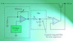
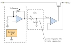
Where the input range of the LDO and its output voltage range will vary—(say) 2.2 to 5.5 V on the input, 1.2 to 4.5 V on the output—your voltage-adjustment mechanism will need some work. Your on-chip voltage reference, dependent on a bandgap reference, can be noisy. For use in cell phones and wireless access terminals (and other low-level RF devices), manufacturers can do you the favor of putting an RC filter on-chip (see figure).
LDOs that use a bandgap voltage reference may need a filter to suppress noise in sensitive RF circuits. (Source: Texas Instruments)
With this particular circuit, the output-voltage requirement is fixed (set for you at the factory), between 1.2 and 4.5 V in 25-mV steps. The output current could be as high as 250 mA, and your dropout will be 120 mA. But your noise specification is less than 10 µV rms.
Minimizing capacitors (their size and value) is a general requirement for power-supply filters. Depending on the on the output level, input and output capacitors can be miniature ceramics (1 µF).
Post-Regulator Filtering
One popular means of minimizing circuit noise is to use a linear regulator in a circuit after a dc-dc converter applies its initial regulation. However, this can also make switching regulators one of the biggest sources of noise in an LDO regulator circuit. While the dc-dc converter can be counted on to narrow the dc voltage-supply rails, additional filtering is required to minimize the output-voltage ripple inherent to dc-dc switching conversions.
You don’t want the ripple noise from the switcher trickling through the power train. For a dc-dc converter, the ripple, related to the frequency of the converter, could be 100 kHz or more, and not easy to filter.
In principle, the linear regulators used in post-regulator switching circuits can be called up to perform a noise-filtering function. The advantages of a two-stage regulator include improved stability and accuracy, a faster transient response, and lowered output impedance.
In practice, switching regulator ripple and current spikes require separate attention ―especially with increasing switching frequency of the dc-dc converter. The effect of ripple is actually magnified whereby the difference between the linear regulator’s input voltage (VIN) and its output voltage (VOUT) is small—a requirement, as mentioned, for power-stage efficiency.
Process technology matters in the fabrication of low-noise parts. Bipolar technology (rather than CMOS) will support high-accuracy, high-precision instrumentation applications in which noise-free voltage rails are required to maximize system performance. These special applications include medical instruments, radio-frequency (RF) transceivers (including mobile handsets), and test-and-measurement equipment.
Low Noise is Key in These Applications
Noise can become problematic in applications such as RF (or wireless network transmitters) and precision measurements. In operation, a variety of precision parts—operational amplifiers, analog-to-digital converters (ADCs), digital-to-analog converters (DACs), and other high-performance analog circuitry—will require low-noise and highly stable power rails.
A part that’s suitable for post-regulation will offer power-supply ripple rejection of 82 dB (behind a 100-Hz switcher) or better than 55 dB (behind a 10 Hz dc-dc). Output-voltage noise is less than 4 µV rms (behind 10-Hz or 100-kHz switchers). Dropout voltage is less than 307 mV at 1 A.
For adjustable regulators, a low-dropout regulator implemented in biCMOS—with a P-channel MOSFET—offers outputs from 0.8 to 6 V, a power-supply rejection ratio (PSRR) of 63 dB at 1 kHz and 57 dB at 100 kHz. Dropout is 170 mV with 1-A regulator output.
Below is a list of the most critical LDO specifications and usable values. Note, picking the right parts for an application could be challenging for designers, as specifications like output voltage range and low noise may require tradeoffs.
• High PSRR: 40 dB+ @ 100 kHz
• Low noise: Less than 20 μV rms
• Low quiescent current (IQ): Less than 15 μA
• Low dropout voltage: 30 mV @ 150 mA out; 125mV @ 2 A out; 115 mV @ 3A
• Small packaging: 1 × 1 mm; 0.65 × 0.65 mm; 0.8 × 0.8 mm
• Wide input-voltage range: 60-V VIN; 100-V VIN; 30-V VIN
• Features: Power-good signal line, capacitor-free operation, reverse-current protection, reverse-voltage protection, soft-start, and output discharge
Looking for parts? Go to SourceESB.


