Synchronous Buck Converter Optimizes EMC, Size, Efficiency at 2 MHz
Download this article in .PDF format
Power-supply design becomes complicated when you’re faced with multiple conflicting specifications. One example is the design of a double-data-rate (DDR) memory supply for an automotive environment. The design objectives are to minimize supply size, maximize efficiency, and minimize electromagnetic interference (EMI) to other systems. Obviously, tradeoffs are involved.
Tradeoffs
The key specification of any switching dc-dc converter/regulator is switching frequency. High frequency is desirable because the inductive and capacitive filtering components can be smaller and less expensive. However, the higher frequencies increase component losses and overall heating.
Furthermore, designers must meet electromagnetic-compatibility (EMC) requirements for automotive applications. Avoiding interference to AM radios is a serious consideration. Switching-frequency choices of 400 kHz and 2 MHz solve this problem. The higher frequency is the most desirable if the efficiency specification can be met, and that depends on converter configuration.
Another decision to make is converter type. For applications requiring a low output voltage with high current and a common ground, a buck converter is a good choice. It takes a higher input voltage and translates it to a regulated lower output voltage with high current capability. This is a good solution for an automotive DDR memory supply.
Buck-Converter Fundamentals
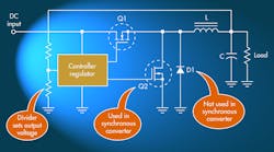
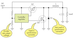
As a refresher, a buck converter is illustrated in the figure. A dc input voltage is switched off and on by MOSFET Q1. A controller circuit sets the switching frequency and duty cycle. When Q1 is on, the input dc is applied to the inductor that initially opposes the input. However, current eventually begins to flow, providing an output to the load and the capacitor. This charges the capacitor.
When Q1 turns off, the magnetic field developed around the inductor during current flow begins to collapse. This induces a voltage in the inductor with a polarity that ultimately forward-biases the commutating or catch diode D1. This allows current to continue to flow in the load.
The diode plays a major role in the efficiency of the circuit. Its typical forward drop of 0.5 to 1 volt is a major loss point. To overcome this problem, a MOSFET with a low on-resistance replaces the diode, reducing the voltage drop to 0.3 V or less. This change creates what’s known as a synchronous buck converter.
A basic buck converter uses a single commutation diode D1 to maintain current flow in the load when Q1 is off. A synchronous buck converter is created by replacing the diode with a low on-resistance MOSFET Q2. The controller optimizes and synchronizes the switching of the two transistors using pulse-width modulation (PWM) to maintain a constant output voltage.
The controller turns this shunt transistor off and on in synchronization with the high-side MOSFET—the two devices are never on at the same time. The shunt transistor is typically integrated with the IC controller chip. ICs are available where both shunt and series MOSFETs are fully integrated into the same package.
For a dc-dc converter and regulator, the controller duty cycle will be varied to compensate for any output voltage increases or decreases. The capacitor provides ripple filtering.
The prime factors affecting efficiency are MOSFET on-resistance, switching frequency, duty cycle, and MOSFET rise-fall times. Inductor ac loss will also impact efficiency. As general rule, a synchronous buck converter is more efficient than a non-synchronous converter, especially at higher current loads.
Optimizing the Design
What’s the secret to balancing all of the design factors in order to optimize efficiency? It basically comes down to controlling the MOSFET switching times. The controller must provide the best duty cycle to maintain the desired output voltage and current. Subsequently, that duty cycle must be coordinated with the shunt MOSFET switching time. Feedback from the load provides the signal for this control.
Other critical considerations include the rise/fall times of the MOSFETs as one transitions from off to on and vice versa, and the minimum input-voltage to output-voltage ratio that determines the minimum on-time of Q1 to provide the desired regulation.
For details of this timing and related factors at higher switching frequencies, check out this reference.
Control Solution
One IC that achieves the desired control is Texas Instruments’ TPS54116-Q1 DDR memory power solution. The TPS54116-Q1 is a dc-dc synchronous buck converter designed to operate at 2 MHz. Its output is 1.5 V with a maximum current of 4 A. An external divider allows for an adjustable output voltage; input voltage range is 2.95 to 6 V. The device also features an integrated 1-A source/sink low-dropout regulator (LDO) for DDR memory termination. Overall efficiency approaches 90%.
Obtaining 2-MHz switching frequency may be desirable, but it’s often difficult to know whether it can be achieved across all operational conditions. Keep in mind that there are always tradeoffs between the size of a dc-dc converter and efficiency. One way to discover the advantages and disadvantages is to order an evaluation module using the previously mentioned IC. It’s designated the TPS54116-Q1EVM-830.
Another approach to designing a converter is to use available design tools such as TI’s WEBENCH. It can help solve switching-power-supply design problems before building a prototype. It enables you to create customized power supplies or dc-dc converters by providing representative power-supply designs and prototyping tools that can be converted and adapted for your own design.


