Download this article in PDF format.
Part 1 of this article provided some general recommendations for designing printed-circuit boards (PCBs) using motor-driver ICs, which require careful PCB layout for proper performance. Part 2 discusses some specific PCB layout recommendations for using typical motor-driver IC packages.
Layout for Leaded Packages
6. SOT-23 and SOIC packages are typically used in low-power motor drivers.
Standard leaded packages, like SOIC and SOT-23 packages, are often used for low-power motor drivers (Fig. 6).
To maximize the power-dissipation capability of leaded packages, Monolithic Power Systems (MPS) uses a “flip-chip on leadframe” construction (Fig. 7). The die is bonded to the metal leads using copper bumps and solder without the use of bond wires. This allows heat to be conducted from the die through the leads to the PCB.
7. A flip-chip on leadframe structure helps maximize power dissipation in leaded packages.
Thermal performance can be optimized by attaching large copper areas to the leads that carry high current. On a motor-driver IC, typically the power, ground, and output pins are attached to the copper areas.
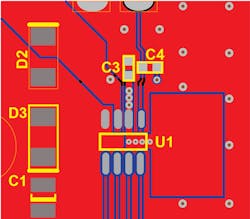
Figure 8 shows a typical PCB layout for a “flip-chip on leadframe” SOIC package. Pin 2 is the device power pin. Notice that a copper area is placed near the device on the top layer, and several thermal vias connect this area to copper on the backside of the PCB. Pin 4 is the ground and is connected to the copper ground pour on the top layer. Pin 3, the device output, is routed to a large copper area as well.
8. Shown is a flip-chip SOIC PCB layout.
Note that there are no thermal reliefs on the SMT pads; they’re connected to the copper areas solidly. This is critical for good thermal performance.
QFN and TSSOP Packages
TSSOP packages are rectangular in shape and use two rows of pins. TSSOP packages used for motor-driver ICs usually have a large exposed pad on the underside of the package that’s used to remove heat from the device (Fig. 9).
9. A TSSOP package often has a large exposed pad on its underside for heat removal.
QFN packages are leadless packages that have pads around the outside edges of the part, as well as a larger pad centered on the underside of the device (Fig. 10). This larger pad is used to extract heat from the die.
10. Pads go around the edges of QFN packages, in addition to having a larger pad centered on the underside for heat extraction from the die.
To remove heat from these packages, a well-soldered connection must be made to the exposed pad. This pad is normally at ground potential, so it can be tied into the PCB ground plane.
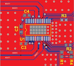
Ideally, thermal vias are directly placed in the pad area. In the example shown in Figure 11, an array of 18 vias is used with a finished hole diameter of 0.38 mm. This via array has a calculated thermal resistance of about 7.7°C/W.
11. This TSSOP PCB layout employs an array of 18 thermal vias.
Normally, finished hole sizes of 0.4 mm and smaller are used for these thermal vias to prevent solder wicking. If smaller holes are required by the SMT process, more holes should be used to keep the overall thermal resistance as low as possible.
In addition to the vias placed within the pad area, thermal vias are placed in areas outside the IC body. In TSSOP packages where copper areas can extend beyond the ends of the package, this provides another path for heat to pass from the device through the top copper layer.
With QFN devices, pads on all four edges of the package prevent the use of copper in the top layer to extract heat. The use of thermal vias is mandatory to pull heat out to either an inner plane or the bottom layer of the PCB.
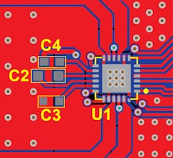
12. Thermal performance of this 4- × 4-mm QFN PCB falls below that of the TSSOP in Fig. 11, because it can only fit nine thermal vias in the exposed pad.
In Figure 12, the PCB layout shows a small QFN (4 × 4 mm) device. Only nine thermal vias fit in the exposed pad area. Because of this, the thermal performance of this PCB is not as good as the TSSOP package shown in Fig. 11.
Flip-Chip QFN Packages
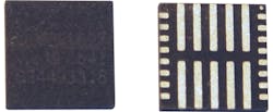
Flip-chip QFN (FCQFN) packages are similar to regular QFN packages, but instead of using wire bonds to connect the die to the package pads, the die is flipped upside down and connected directly to the pads on the underside of the device. The pads can be placed opposite the heat-generating power devices on the die, so they’re often arranged as long stripes instead of small pads (Fig. 13).
13. Flip-chip QFN (FCQFN) packages connect directly to the pads on the underside of the device.
These packages use rows of copper bumps on the surface of the die, which are then bonded to the leadframe (Fig. 14).
14. FCQFN packages use rows of copper bumps on the surface of the die, which are subsequently bonded to the leadframe.
Small vias can be placed within the pad areas, similar to what’s done with regular QFN packages. On multi-layer boards with power and ground planes, vias can directly connect these pads to planes. In other cases, copper must be attached to the pads directly to draw heat away from the IC into larger copper areas.
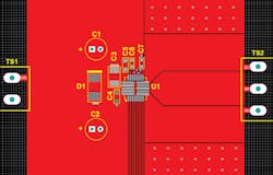
Figure 15 shows a PCB layout for an MP6540 power-stage IC. This device has long pads for power, ground, and the three outputs. Note that the package is only 4 × 4 mm.
15. Here’s a FCQFN PCB layout for an MP6540 power-stage IC.
The copper area to the left of the device is the power input. This large copper area is directly connected to the two power pads of the device.
The three output pads are connected to copper areas to the right of the device. Note how the copper area is expanded as much as possible just after exiting the pad. This provides good heat transfer from the pad to the ambient air.
Also note the rows of small vias within two of the pads at the right side of the device. These pads are connected to ground, and a solid ground plane is placed on the backside of the PCB. These vias are 0.46 mm in diameter with a finished drill hole of 0.25 mm. The vias are small enough to fit within the pad area.
Careful PCB layout is necessary to implement successful designs using motor-driver ICs. This article has presented some practical suggestions to help PCB designers achieve good electrical and thermal performance.
