This article is part of TechXchange: Power Supply Design
Download this article in PDF format.
Over the past several decades, one by one, analog electronic gadgets such as cassette tapes/players, VHS tapes/players, film cameras, CRT televisions/monitors, etc., have been dumped by the truckload in electronic recycling graveyards. Though not yet in the same category as a dinosaur, they’re all surely to wind up under the same roof—namely, a museum.
So far, analog power supplies have miraculously, and unexpectedly, been able to escape the misery. However, the inevitable will come, as attested to by the appearance of drones and driverless vehicles—all products of digital technologies.
In light of this trend, what should professionals well-trained in conventional analog circuits do to avoid being placed in the analog museum?
Tumble to Digital
Early on, what had happened to those antiquated apparatus certainly caught the attention of many corporate CEOs and business planners. Quite a few, including TI, Motorola, and, in particular, those who have stakes in power conversion, actually took steps to initiate the transition to digital techniques. Several companies thought, banking on their success on digital motor-control products, it should be easy to rein in the analog power converters with their existing devices and capabilities. However, the expectation failed to materialize.
It turns out that the know-how derived from motor control focuses on different areas that contrast from digital power conversion. In essence, the techniques (e.g., d-q decomposition, space-vector-modulation, etc.) developed via digital motor control can be viewed as versions of a more sophisticated sequential pulse-width modulation (PWM) intended to generate perfect motor (shaft) rotation. Digital power conversion, on the other hand, sets its priority on feedback error processing via digital means instead of analog amplifiers. Generation of PWM is less of a concern.
Roadmap to Digital
So, then, what are the procedures required to move conventional analog power converters to the digital realm? Prior to answering that question, though, perhaps one other question should be asked first: What part(s) of an analog power converter should, or can, be replaced by digital devices?
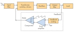
1. Block diagram of a typical switch-mode dc-dc converter.
The decision must be made by carefully examining the architecture, or the structure, of a traditional analog power converter—a switch-mode dc-dc converter (Fig. 1)—to expedite the discussion without omitting crucial points.
Either by coincidence or by magic, Fig. 1 seems to partition the converter in two subgroups: feedforward consisting of VIN, input filter…output filter; and feedback containing feedback scaling, error amplifier, comparator, and clock.
Clearly, those blocks and associated elements grouped in the forward path simply can’t be replaced by digital devices, since it involves real energy storage, and exchange, in electrical or magnetic form. On the contrary, the feedback path is replaceable.
Overall, the feedback path has five elements: feedback scaling, reference command, error amplifier, ramp clock, and PWM comparator. Both the feedback scaling and reference command are simple numbers and are easily replaced by digital words. The ramp clock is also a simple block that’s easy to replace digitally.
The PWM comparator requires more intricate discussion on whether or not it should be replaced. In theory, it’s quite simple to perform digital PWM operation with a digital comparator or lookup table. It’s not a feasibility issue, but rather a necessity debate. Very few switch-mode power converters operate beyond 500 kHz. At that switching frequency, a PWM duty cycle ranging from 5% to 70% translates to a 100- to 1,400-ns pulse width.
Modern digital hardware can easily provide clock resolution at 1 ns (GHz). However, high-speed MOSFET switches exhibit typical turn-on rise time/turn-off fall time on the order of 10 to 20 ns. In addition, power-converter output filters generally are designed to extract dc (Fourier) component with low bandwidth less than a few kilohertz. In other words, delta pulse width in the neighborhood of ±10ns at high speed simply doesn’t register. Unable to offer practical benefit, digital PWM perhaps should sit on the sideline.
The remaining error amplifier is definitely the best candidate for digital replacement. The question is how to go about it.
Navigate to Digital Filter
First, let’s accept a blunt reality: Digital filters can’t be grabbed from thin air. Conventional analog error amplifiers allow designers less inclined in analytic means to play with, or tweak, RC components surrounding the amplifier. Playing with, or tweaking, coefficients of digital filter functions in the z-transform is no longer an option.
The digital filter must be derived from the analytical expression of a known analog counterpart that has properly stabilized a control loop. To obtain the pertinent digital filter, the following steps must be taken:
1. Based on analytical procedure, design, build, and test the feedforward portion of a power converter.
2. Select a feedback scaling factor, kf.
3. Select a nominal PWM gain, Gpwm (%/V), derived from the ramp waveform.
4. Extract power-stage duty-cycle-to-output gain, Gvd(s), and input source-to-output gain, Gvg(s), based on the state space averaging with both the input and output filter included in the procedure.
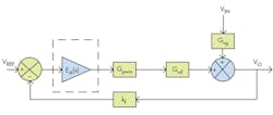
5. Steps 1-4 enable designers to place Fig. 1 in control block diagram form (Fig. 2).
2. Control block diagram form of a typical switch-mode dc-dc converter (Forward converter with voltage-mode control).
6. Partition the control block diagram into two groups with the error amplifier, EA(s), standing alone, and the rest named M(s) for modulator.
7. Formulate and compute the modulator gain M(s) = kfGpwmGvd(s).
8. Refer to the M(jω) plot, and at a selected, desired crossover frequency fc (equivalent to the closed-loop bandwidth), read out the modulator gain, Mdb(ωc), and the modulator phase, θM(ωc), in degrees.
9. Set the desired phase margin, θm(ωc), at fc.
10. From θM(ωc) and θm(ωc), factoring in the negative sign of feedback, compute the phase boost, θb(ωc), required.
11. Select a type-II, or type-III amplifier, given step 10. Then compute the pole-zero separation factor, k.
12. Force the error amplifier selected to compensate the modulator gain. −Mdb(ωc) and pole-zero separation factor k allow the designer to compute RC components needed for the amplifier.
13. Express the error-amplifier transfer function, EA(s), in the s-domain and in symbolic standard form, type-II −(as+1)/[bs(cs+1)], or type-III –(as+1)2/[bs(cs+1)2].
14. Compute the loop gain T(s) = EA(s)M(s) and verify that it does cross fc with the desired phase margin.
15. Plot EA(jω) and select a sampling frequency, fs , where EA(jωs) ≈ −30 db.
16. Invoke the bilinear transform and plug in s = C(1-z-1)/(1+z-1) in EA(s) standard form without the “minus” sign, C = 2fs.
17. Manipulate EA(z) and place it in a standard z-transform (a0+a1z-1)/(1+b1z-1+b2z-2), or (a0+a1z-1+ a2z-2)/(1+b1z-1+b2z-2+ b3z-3).
18. The z-transform obtained in step 17 is the digital filter being sought.
Work Out a Forward Converter Example
The digital power supply still remains a vast subject for more studies, and a rich environment for testing advanced techniques with unimaginable capacity of elevating those already in existence. Such a high bar exceeds any single individual’s resourcefulness. With that in mind, the following outline expands on the above, discussing an isolated forward dc-dc converter operating in continuous conduction mode (CCM) with voltage-mode control:
1. Specification: 43< Vin = 48 <52; Vo = 5.2; Po = 100 W; δvo = 1%; δio = 10%; fs = 125 kHz…
- Select output filter bandwidth Fbw = 2 kHz; maximum duty cycle Dmx = 0.4 at Vin_mn; therefore, transformer turn ratio n = Ns /Np = Vo/(Vin_mn Dmx) = 0.3; Ns = 2, Np = 7.
- Select output capacitor and output inductor
- Follow Ref. 1 and select output filter shunt damping in order to avoid light load peaking.
- Establish the reflected load impedance looking into the primary winding.
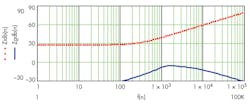
- Design an input filter such that its output impedance is much smaller than |Zip(s)|, for example (Fig. 3).
3. Input filter source impedance (solid) and output filter input impedance (dot) interaction.
2. Feedback scaling factor, kf = VREF/Vo, is in general a simple voltage divider. It should precede a unity gain buffer and be isolated from error amplifier’s pole-zero placement.
3. PWM can be implemented in several ways: positive ramp, negative ramp, and dual ramp. There are also multiple choices for modulation edges: trailing edge, leading edge, or both (Fig. 4). However, if the carrier and modulating signals interchange their entry port at the comparator input, equivalent to using the complement of modulated output, those terminologies may become blurred.
4. PWM schemes include (from left to right) positive trailing edge, negative leading edge, and dual edge.
For this example, the positive ramp with trailing-edge modulation—the most popular scheme—is chosen. The modulation gain is Gpwm ≈ 0.98/(VH − VL). A 2% dead zone is enforced.
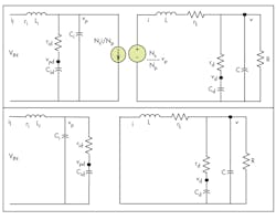
4. Place the power stage circuit in switch-ON and switch-OFF configurations (Fig. 5).
5. Two states of a power stage are switch-ON and switch-OFF.
5. Given state column vector x = (i, v, vd, i1,vp, vpd)T, follow Prof. Middlebrook’s state-space averaged technique2 and derive six state transition matrices: A1, B1, C1, for ON-state; A2, B2, and C2 for OFF.
6. With those matrices, find the steady-state duty cycle D, calculate the steady-state vector X, and then develop the power-stage gain Gvd(s).
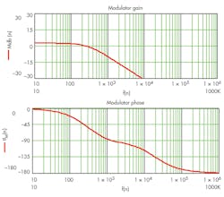
7. Referring to Fig. 2, compute the modulator gain M(s) = kfGpwmGvd(s) and plot both magnitude Mdb =20log(| M(ω) |) and phase θM(ω) (Fig. 6).
6. Modulator gain and phase.
8. Select fc = 2 kHz, read Mdb(fc) = −16 db, θM(fc) = −94°.
9. Set desired phase margin, θm(fc) = 60°.
10. Phase boost required θb(fc) = θm(fc) − [ θM(fc) + 90º] = 64°.
11. Select type-III amplifier given step 10; calculate pole-zero separation factor.
12. Refer to Ref. 3 to compute RC components for the type-III amplifier (Fig. 7).
7. Type-III amplifier, where A(s) = open loop gain.
13. The analog error-amplifier transfer function, EA(s), in the primitive form:
and in the standard form:
Refer to Ref. 4 (appendix), or many other DSP books, to transform the analog amplifier gain from primitive form to standard form.
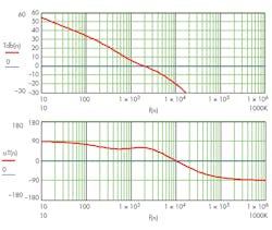
14. Loop gain T(s) = EA(s)M(s). As shown, it does cross fc—the frequency at which intercepts the zero-db blue line—with desired phase margin (Fig. 8).
8. Loop gain and phase.
15. Plot |EA(jω)|. Select a sampling frequency, fs , where EA(jωs) ≈ - 30db, since significant activity is still observed. fs = 1MHz .
16. C = 2 MHz; plug in s = C(1 − z-1)/(1 + z-1) in EA(s) standard form without “minus” sign.
17. Rearrange EA(z) and place it in standard z-transform. Both an and bn turn out to be extremely complicated functions of RC components obtained in steps 12 and 13. In this example, they are:
Because six decimal points are retained to express all coefficients appearing in the digital error amplifier; digital-filter performance is extremely sensitive to them. Designers are cautioned not to make any unwitting truncation of those numbers derived from the procedure.
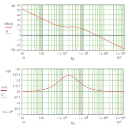
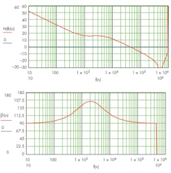
18. The z-transform obtained in step 17 is the digital filter being sought. It can be verified by plotting EA(z); magnitude and phase.
Comparing Figures 9 and 10, one sees differences at high frequency.
9. Analog error-amplifier gain and phase.
10. Digital error-amplifier gain and phase.
Implementation
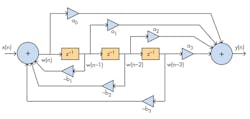
The digital amplifier/filter obtained in step 17 can be implemented in many ways. Determining the optimal method involves various factors, such as number of multiplications, number of delay operator z-1s, etc. The author chose the direct form-II (Fig. 11), based on intuition and for its straightforward connection with mathematical expression. There’s still a lot of room beyond an individual’s capability, though.
11. Direct form-II digital filter implementation.
One more critical observation easily hidden from view, but embedded in mathematics, comes from how the expression is written for the error amplifier output. Referring to Figure 7, it’s commonly expressed as:
However, it can rewritten as
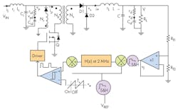
In other words, the error amplifier, or the digital filter, operates on the difference only. Meanwhile, the command reference, VREF, sets up the dc operating point. And that is how the digital filter replaces the analog error amplifier (Fig. 12).
12. A forward SMPS with digital filter takes the place of analog error amplifier.
The PWM remains in analog form for reasons outlined above. Furthermore, the best place for an analog-to-digital converter is after the subtraction, VREF − kfvo, considering the full-scale utilization of analog-to-digital operation.
Conclusion
Digital technologies have, in a fundamental way, altered the way electronic apparatus are designed and built. That trend will keep advancing. Eventually, the majority of switch-mode power supplies/processors (SMPS) will fall under the same umbrella.
This article, meant not to be an exhaustive exposition of digital power-converter design, outlines a systematic procedure believed to be effective in bringing conventional SMPS based on analog control to ones with digital feedback. The procedure was called upon to treat a SMPS, a forward converter in CCM with voltage-mode control. Other switch-mode power converters operating in CCM with current-mode control, or in discontinuous conduction mode (DCM) with voltage/current-mode, require additional modifications.
Several skill sets are required to perform the outlined tasks: Control system analysis based on analog s-domain approach; analytical identification and extraction of key control function, digital signal processing and conversion of s-domain function to z-domain; and digital implementations based on a mix of software and hardware.
Given the scope of such multifaceted tasks, it’s unreasonable to expect an individual to master them all. A team consisting of an analog analyst, DSP expert, and hardware engineer stands a better chance to get the job done well.
Read more articles in TechXchange: Power Supply Design
References:
1. “Pulse Width Modulated DC/DC Converters,” ISBN 0-412-10541-1, 1997.
2. “Modeling, Analysis and Design of Switching Converters,” Slobodan Cuk; R.D. Middlebrook; NASA CR-135174; TRW A72042-RHBE; TRW D04803-CFCM.
3. “Switch-mode Power Converters,” ISBN-13: 978-0-12-088795-8, 2005.
4. “Power Converters with Digital Filter Feedback Control,” ISBN: 978-0-12-804298-4, 2016.
