Portable electronic game consoles present the challenge of delivering high graphics quality and a realistic gameplay experience within the constraints of the limited energy provided by battery-operated devices (Fig. 1). The adoption of multi-core central processing units (CPUs) and powerful graphics processing units (GPUs), on the processing side, and multi-phase switching regulators, on the power-supply side, go a long way toward achieving high levels of performance for sustained amounts of time.
1. Today’s portable game consoles need more power to handle the graphics.
This article reviews the challenge of powering a portable game console and presents a configurable, high-current, high-efficiency, multi-phase switching regulator that well-suited for this application.
Multi-core CPUs for portable games enable complex, immersive, and realistic electronic gaming features like real-time physics and real-time texture generation within the limited energy available in portable applications. Multiple concurrent tasks can be executed faster when multiple cores are available. The distribution of multiple complex tasks across different cores results in reduced power losses as each CPU runs at a lower frequency to complete its reduced task.
GPUs for portable gaming handle ever-increasing pixel-processing loads while remaining within mobile power budgets with the help of advanced power-management techniques. System-level and local clock-speed management like dynamic voltage and frequency scaling (DVFS) helps minimize GPU power consumption and delivers graphic performance approaching that of a desktop console.
When the docking station isn’t available, portable game consoles rely on a single-cell lithium battery to power the CPU, GPU, and DRAM module. Typically, a lithium battery with 4-Ah capacity should sustain five hours of operation, adding up to an average current draw of 0.8 A, and peak currents many times higher. Each of these smart loads (CPU, GPU, DRAM) must be powered by versatile switching regulators that can efficiently deliver current over a range spanning from a fraction to tens of amperes.
The Multi-Phase Buck Converter
Following a similar strategy outlined for multi-core CPUs, a multi-phase buck (step-down) converter is the best choice to power these smart loads. Dividing the current between four phases that are equally spaced in time across one clock period offers several advantages compared to a single-phase architecture.
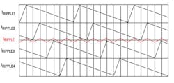
2. Quad-phase output ripple-current cancellation.
First, the four interleaved phases assure output ripple-current cancellation as shown in Figure 2. Notice how the total ripple-current frequency is four times that of a single phase, while the amplitude is a quarter. Therefore, high-frequency, low-amplitude ripple current is obtained at a relatively low frequency operation of each phase. Lower ripple current means fewer capacitors are needed on the output, resulting in a smaller bill of materials.
Secondly, a multi-phase scheme is more efficient than a single-phase scheme. The latter, by running at four times the frequency of the quad phase, can also achieve low current ripple but at higher switching losses. In this case, the two schemes have an equal number of transitions within one period, but the quad-phase converter transitions carry a quarter of the current of the single-phase converter.
Third, the multi-phase architecture results in the need for fewer input capacitors—the total input current, within one period, is the sum of four out-of-phase currents. Here, spreading the total input current over time reduces its RMS value, compared to single-phase operation, which allows for a smaller input current ripple filter.
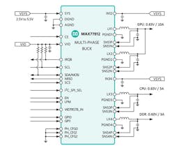
Addressing this need, Maxim Integrated developed the MAX77812 (Fig. 3), a configurable, single-to-quad-phase, single-to-quad-output high-current, buck (step-down) converter. High efficiency, a small PCB solution footprint, high output-voltage accuracy, fast transient response, and a fast serial interface option make the device well-suited for powering CPUs and GPUs in portable game consoles.
3. Here, the MAX77812 is set up in a 2+1+1 user-selectable phase configuration.
The MAX77812’s flexible architecture allows for user-selectable phase configurations such as 4 (one four-phase output), 3 + 1 (two outputs, one tri-phase and one single-phase), 2 + 2 (two two-phase outputs), 2 + 1 + 1 (three channels, one two-phase, two single-phase), and 1 + 1 + 1 + 1 (four single-phase outputs).
Single-Chip Processing System Power
By choosing the proper configuration, a single MAX77812 can power the processing block in portable game consoles. In Fig. 3, a 2 + 1 + 1 configuration has been selected to power the GPU, CPU, and DDR memory.
The flexible architecture of the MAX77812 makes the device easy to reuse. For example, customers may initially choose a 2 + 1 + 1 phase configuration: two phases for GPU, one for CPU, and one for DRAM. Later on, they may realize that the GPU needs more current. With the device, they have the option to switch to a 3 + 1 configuration: three rails for the GPU and one rail for the CPU. This is done by simple pin-strapping without part number changes. The addition of a single-phase buck converter for the DRAM is still necessary, but it’s much less painful than redesigning the GPU multi-phase buck converter. The regulator’s flexibility helps speed up design and qualification, reducing time to market.
The MAX77812 can be configured as a 30-MHz SPI high-speed serial interface to provide flexible control of each regulator. DVFS operation and output-voltage ramp rate control enable rapid output voltage adjustment to optimize performance in all system operating states. The device also features an I2C-compatible, two-wire serial interface.
During DVFS operation, the buck converter responds to a command to quickly change the output voltages to new target values. The high peak-current limit, coupled with low inductance and small output capacitance, allow the device to operate with high slew rates.
DVFS operation can cause very high current peaks of short duration. For example, an output loaded by a 100-µF capacitor will require a current of 6 A to raise its value by 60 mV in 1 µs (60-mV/µs slew rate). This, together with the high variability of the CPU and GPU current profiles, explains the necessity for the voltage regulator to have a maximum current rating as high as 20 A.
High Accuracy Saves Power
As power goes with V2/R, a 1% loss in accuracy results in 2% wasted power. That’s the same as taking the efficiency curve and lowering it by 2% points. The MAX77812’s high initial setpoint accuracy (±0.5%) and phase differential remote-sense feedback enable very tight dc and ac accuracy at the point of load.
To save power, the MAX77812 operates in skip mode (SKIP) at light loads and automatically transitions to pulse-width modulation (PWM) at heavy loads (auto-mode). This operation mode tradeoff is slow transient response, which results in high output-voltage transient spikes. A low-power skip mode (LP SKIP) is also available for even lower power consumption in light load operation.
The output of a slow voltage regulator will dip under a positive transient load and need to be positioned higher to assure that the load receives the minimum voltage necessary to operate. This results in wasted power and greater heat generation, ultimately ending in less battery life. To alleviate that problem, Maxim’s Enhanced Transient Response (ETR) monitors the output voltage and forces the output stage appropriately in presence of high slew rate.
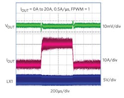
If the system can predict the application of a heavy load, the best strategy is to force PWM mode (FPWM = 1) just ahead of a load step change. This way, the allowance made for the output-voltage droop can be reduced to a minimum and the output voltage can be set as low as possible, improving efficiency.
The transient response of the MAX77812 in forced PWM mode is demonstrated in Figure 4.
4. Shown is the transient response for the MAX77812 in force PWM.
Efficiency Advantage
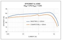
The enhanced features of the MAX77812’s integrated power MOSFETs result in higher efficiency versus that of competitive quad-phase solutions. The comparison in Figure 5 (2520 size inductors) shows up to 7% (15 A) greater efficiency versus a competitor device.
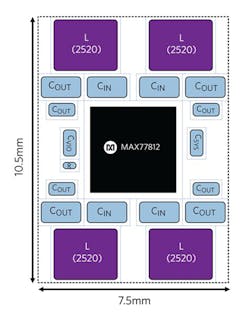
The MAX77812 has a miniature PCB footprint, occupying only 78.75 mm2, replete with small inductors and capacitors (Fig. 6). A programmable current limit minimizes the inductor sizes based on the system’s actual requirements. Packaging for the device is a 64-bump, 0.4-mm-pitch WLP package with a height of 0.64 mm (typical).
6. The MAX77812’s PCB footprint is a mere 78.75 mm2.


