Semiconductor manufacturers have developed innovative production techniques that enable the integration of multiple components and a dc-dc converter IC die into a single module. Producing such a dc-dc module involves providing the following:
- Protection for its associated die from the surrounding environment.
- An electronic pathway from the die to its external circuits.
- A method for attaching the module to a PCB.
- Enough I/O pins to accommodate complex circuits.
- The ability to integrate multiple components into the module.
- A means for module heat removal.
Mounting on a PCB
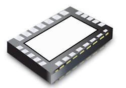
The module will be mounted on a PCB so it should use a method employed by semiconductors. One mounting method is similar to the QFN flat lead semiconductor package that physically and electrically connect semiconductors to PCBs. Perimeter pads on the QFN package bottom provide electrical connections to the PCB (Fig. 1). Other flat no-lead semiconductor packages that could be used are the micro leadframe (MLF) and small-outline no leads (SON).
1. A QFN package has solder pads on the bottom along with an exposed pad to aid in heat removal.
The QFN package uses perimeter I/O pads to ease PCB trace routing, and the exposed copper die-pad technology offers good thermal and electrical performance. These features make the QFN an ideal choice for many module applications where size, weight, and thermal and electrical performance are important. The QFN package format offers benefits of:
- Reduced lead inductance
- Small sized "near chip scale" footprint
- Thin profile
- Low weight
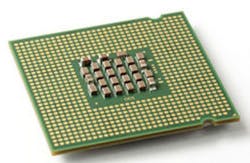
If there’s a need to provide a large number of I/O pins, you could use a land-grid-array (LGA) packaging technique with a rectangular grid of contacts on the underside of the module (Fig. 2). Not all rows and columns of the grid need to be used. LGA modules can fit either in a socket or be soldered down using surface-mount techniques.
2. An LGA array has a grid of contacts that’s connected to a grid of contacts on a PCB.
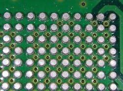
The ball grid array (BGA) is another option to obtain multiple I/O pins (Fig. 3). It’s a surface-mount device used to permanently mount semiconductors. A BGA can provide more interconnection pins than can be put on a dual in-line semiconductor package.
3. The BGA uses a grid of solder balls to conduct electrical signals to/from the PCB.
BGA solder balls can be spaced evenly apart without accidentally bridging them together. The solder balls are first placed on the bottom of the module in a grid pattern and then heated. By using surface tension when melting the solder balls, the module can be aligned with the circuit board. The solder balls cool and solidify with an accurate and consistent distance between them.
Shrinking the Power Converter
About five years ago, semiconductor manufacturers began producing dc-dc converter modules that include components integrated into the module rather than external to the device. Besides allowing space for integrated components, the new production techniques had to be cost-effective. Inductors were one of the first passive components inside the module. This was made possible by operating at a high enough switching frequency to allow for a small physical size inductor.
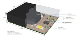
Going beyond just the inductor is a new generation of devices integrated more components. An example is the LTM8058 μModule regulator pioneered by Linear Technology, now Analog Devices (Fig. 4). This module integrates switching controllers, power FETs, inductors, and all supporting components in a conventional BGA format module. The module requires only external input and output capacitors.
4. Internal construction of the LTM8058 MicroModule (Analog Devices) includes an isolated dc-dc converter that provides 2.3- to 13-V output at 440 mA. It’s housed in a 9- × 11.25- × 4.92-mm BGA module.
Currently, the μModule with the highest-rated output current is the LTM4639, which is a complete 20-A output, high-efficiency, switch-mode, step-down dc-dc regulator. Included in the package are the switching controller, power FETs, inductor, and compensation components. Operating over an input voltage range from 2.375 to 7 V, the LTM4639 supports an output voltage range of 0.6 to 5.5 V, set by a single external resistor. Only a few input and output capacitors are needed.
One way to cool the module is to use the PCB itself to spread the power dissipated within the module. This can be done by placing vias underneath and around the module to distribute heat throughout the layers of the PCB. Vias act as very good electrical conductors to interior planes, and serve as heat pipes to allow the PCB to act as a heat sink.
For the best performance and reliability, the module should be operated as cool as possible, so that the best design has as many vias that can fit the module’s footprint. Each via, however, starts as a hole drilled into the board, which reduces the amount of copper present on the PCB layers for electrical conduction. It’s possible to have too many vias, so follow your organization’s design guidelines.
Analog Devices packaging pushed component integration even further with the LTM4661, a µModule synchronous boost converter that takes advantage of small size and a minimum number of external components, allowing it to fit into small spaces. Its 6.25- × 6.25- × 2.42-mm BGA module incorporates a dual-phase switching dc-dc controller, power MOSFETs, inductors, and supporting circuit components. Its only external requirements are three capacitors and one resistor that complete the design. It’s specified for –40 to 125℃ operation. The high level of integration of μModule regulators simplifies the task of PCB design.
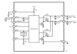
The design strategy for the LTM4661 (Fig. 5) was to minimize the number of external components by incorporating several in the device, including:
- The 28k switching frequency-setting resistor
- The 100k resistor internal and 31.6k external feedback resistors (set VOUT)
- Internal frequency-compensation network
- Four power MOSFETs
- Two inductors (because the LTM4661 internal architecture is a dual-output, dual-phase synchronous boost regulator)
Texas Instruments (TI) employed its new manufacturing techniques for two types of its nano-modules: MicroSiP and MicroSiL. The MicroSIL includes just the inductor, and MicroSiP, which is a true all-in-one solution, features the input capacitor, output capacitor, and inductor. MicroSiL modules have a QFN type of mounting, including a thermal pad that helps get the heat out of these higher-current MicroSiL devices. MicroSiP devices operate at lower currents. Most MicroSiPs are 1 mm maximum height, though some are 1.1mm. MicroSiL devices typically have more height due to the taller inductor used for higher currents.
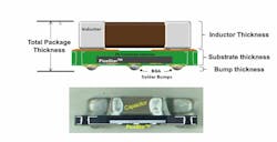
Looking at the MicroSiP, shown in Fig. 6, we can see its green FR-4 laminated substrate with the PicoStar dye; the silicon die is embedded inside. In addition, there’s an inductor on top; the height of the BGA solder bump on bottom determines the MicroSiP size.
6. MicroSiP devices are constructed on a PCB substrate, with the chip inductor and ceramic capacitors soldered on top and BGA solder bumps on the bottom.
MicroSiP has a smaller solution size than the MicroSIL. When you stack the components vertically, as opposed to side by side on the PCB, it reduces the x and y size. The height, of course, increases a little bit when you stack the components, but this isn’t important for many applications. There’s about a 45% smaller x, y size with a MicroSiP compared with an equivalent discrete solution.
Integrating all of the components into one design gives a repeatable and expected EMI and noise performance compared with a traditional PCB layout. And this is true on different systems and different projects.
Nano-Module Provides 1A Output
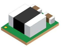
The LMZM23601 is a MicroSiP step-down dc-dc converter that converts a 4- to 36-V dc input to a lower dc voltage with a maximum output of up to 1 A. This nano-module includes the VCC capacitor, boot capacitor, and inductor. The device is available on tape and reel and is pick-and-place compatible (Fig. 7).
7. The LMZM23601 is a 10-pin, 3.0- × 3.8- ×1.6-mm nano-module that provides a complete fixed 3.3- or 5-V output with 1-A output. Adding input and output capacitors results in a 27-mm2 footprint.
The LMZM23601 requires very few external components for a complete dc-dc converter. At 3.3 V or 5 V, the fixed output voltage option requires adding only an external input and an output capacitor. An adjustable output voltage version makes it possible to set the output between 2.5 and 15 V, using two additional feedback resistors.
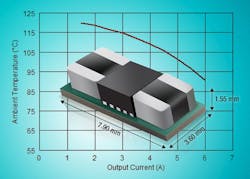
TI also introduced a 5.5-V step-down module that delivers true, continuous 6-A output current with up to 95% efficiency (Fig. 8). The TPSM82480 dc-dc module integrates power MOSFETs and shielded inductors into a tiny, low-profile footprint for space- and height-constrained applications, such as point-of-load telecommunications, networking, and test-and-measurement power supplies.
8. Characteristics of Texas Instruments’ TPS82480 6-A dc-dc nano-module.
TI’s highly-integrated TPSM82480 maintains the required 6-A output current over the full temperature range without additional airflow. This is accomplished using a two-phase control topology that shares the load between the phases to ensure high efficiency and balanced operation. Additional features include adjustable soft-start, voltage select (VSEL) to support multiple processor stages, and a power-good indicator.
The 24-pin QFM module is similar to the QFN, except it has a different pad layout.
Ceramic Power Modules
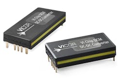
Vicor employs a different module construction. Its ChiP (Converter housed in Package) platform provides a ceramic dc module (DCM) that leverages advanced magnetic structures integrated within high-density interconnect substrates with power semiconductors and control ASICs (Fig. 9). ChiPs provide superior thermal management and high power density.
9. Vicor’s DCM family of wide input range (43- to 154-V input) 3623 (36 × 23 mm) ChiPs feature dc output voltages of 3.3 to 48 V and power levels up to 240 W.
The ChiP module is an isolated, regulated dc-dc converter that can operate from an unregulated, wide-range input to generate an isolated dc output. With its high-frequency zero-voltage switching topology, the DCM converter consistently delivers high efficiency across its entire input voltage range.
