There may be a new player in the semiconductor world, and it comes in the form of gallium-oxide technology. The material could assume a key role in improving electric vehicles, solar power, and other forms of renewable energy, according to Uttam Singisetti, PhD, associate professor of electrical engineering in University of Buffalo’s (UB) School of Engineering and Applied Sciences. He says, “We need electrical components with greater and more efficient power-handling capabilities. Gallium oxide opens new possibilities that we cannot achieve with existing semiconductors.”
The electronics industry is running out of ways to maximize silicon as a semiconductor, which is why researchers are exploring other materials such as silicon carbide, gallium nitride, and gallium oxide. Gallium oxide has poor thermal conductivity, but its bandgap (about 4.8 electron volts, or eV) exceeds that of silicon carbide (about 3.4 eV), gallium nitride (about 3.3 eV) and silicon (1.1 eV).
Bandgap measures how much energy is required to jolt an electron into a conducting state. Systems made with high-bandgap material can be thinner, lighter, and handle more power than systems consisting of materials with lower bandgaps. Also, high bandgap makes it possible to operate these systems at higher temperatures, reducing the need for bulky cooling systems.
5-µm-Wide Ga203 MOSFET
Professor Singisetti and his students (Ke Zang and Abhishek Vaidya) fabricated a metal-oxide-semiconductor field-effect transistor (MOSFET) made of gallium oxide that’s 5 µm wide. A sheet of paper is about 100 µm wide.
The transistor has a breakdown voltage of 1,850 V, which more than doubles the record for a gallium-oxide semiconductor, the researchers say. Breakdown voltage is the amount of electricity required to transform a material (in this case, gallium oxide) from an insulator to a conductor. The higher the breakdown voltage, the more power the device can handle.
Because of the transistor’s relatively large size, it’s not ideal for smartphones and other small gadgets, says Singisetti. But it could be useful for regulating energy flow in large-scale operations such as power plants that harvest solar and wind energy, as well as electric vehicles including cars, trains, and aircraft.
“We’ve been boosting the power-handling capabilities of transistors by adding more silicon. Unfortunately, that adds more weight, which decreases the efficiency of these devices,” says Singisetti. “Gallium oxide may allow us to reach, and eventually exceed, silicon-based devices while using less material. That could lead to lighter and more fuel-efficient electric vehicles.”
For that to happen, however, a few challenges must be addressed, he says. In particular, gallium-oxide-based systems must be designed in ways to overcome the materials’ low thermal conductivity.
This research was supported by the National Science Foundation, the State University of New York’s Materials and Advanced Manufacturing Network of Excellence, and the University at Buffalo Institute for Research and Education in eNergy, Environment and Water (RENEW).
More Gallium-Oxide Research
Other researchers are working with gallium oxide. In an article published in Applied Physics Letters, from AIP Publishing, authors Higashiwaki and Jessen outline a case for producing microelectronics using gallium oxide. The authors focus on field-effect transistors (FETs), devices that could greatly benefit from gallium oxide’s large critical electric field strength. a quality that Jessen said could enable the design of FETs with smaller geometries and aggressive doping profiles that would destroy any other FET material.
“One of the largest shortcomings in the world of microelectronics is always good use of power: Designers are always looking to reduce excess power consumption and unnecessary heat generation,” says Gregg Jessen, principal electronics engineer at the Air Force Research Laboratory. “Usually, you would do this by scaling the devices. But the technologies in use today are already scaled close to their limits for the operating voltage desired in many applications. They are limited by their critical electric field strength.”
The material’s flexibility for various applications is due to its broad range of possible conductivities—from highly conductive to very insulating—and high-breakdown-voltage capabilities due to its electric field strength. Consequently, gallium oxide can be scaled to an extreme degree. Large-area gallium-oxide wafers can also be grown from the melt, lowering manufacturing costs.
“The next application for gallium oxide will be unipolar FETs for power supplies,” says Jessen. “Critical field strength is the key metric here, and it results in superior energy density capabilities. The critical field strength of gallium oxide is more than 20 times that of silicon and more than twice that of silicon carbide and gallium nitride.”
The authors discuss manufacturing methods for Ga2O3 wafers, the ability to control electron density, and the challenges with hole transport. Their research suggests that unipolar Ga2O3 devices will dominate. Their paper also details Ga2O3 applications in different types of FETs and how the material can be of service in high-voltage, high-power and power-switching applications.
“From a research perspective, gallium oxide is really exciting,” Jessen said. “We are just beginning to understand the full potential of these devices for several applications, and it’s a great time to be involved in the field.”
First Gallium-Oxide MOSFETs
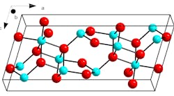
The first successfully demonstrated gallium oxide normally off MOSFET was disclosed by FLOSFIA in Japan. This is groundbreaking work, since it has been considered challenging to produce a normally off MOSFET. FLOSFIA plans to manufacture corundum (a crystal structure) α-Ga2O3 power devices, the GaOTM series, starting from a Schottky barrier diode (SBD) in TO-220 and then a MOSFET.
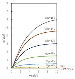
1. I-V curve of a normally off Ga2O3 MOSFET.
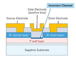
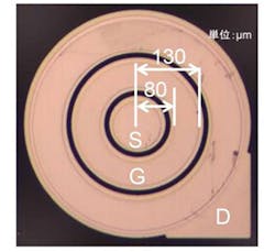
The first α-Ga2O3 normally off MOSFET (Fig. 1) consists of an N+ source/drain layer, p-type well layer, gate insulator, and electrodes (Figs. 2 and 3). The gate threshold voltage extrapolated from the I-V curve was 7.9 V. The device is made of a novel p-type corundum semiconductor that functions as an inversion layer. There was no theoretical study predicting p-type material that’s compatible with n-type Ga2O3 until the team discovered p-type Ir2O3 in 2016. Therefore, it has been considered very difficult to realize a normally off MOSFET.
2. Cross-sectional device schematic.
3. Optical micrograph of anormally off Ga2O3 MOSFET.
FLOSFIA Inc., headquartered in Kyoto, Japan, is a spin-off from a research of Kyoto University, specializing in film-formation by mist chemical vapor deposition (CVD). Making use of physical properties of gallium oxide (Ga2O3), FLOSFIA is devoted to the development of low-loss power devices. The firm succeeded in a development of a SBD with the lowest specific on-resistance of any type currently available (through an internal investigation), realizing technologies linked to power loss reduction that’s reduced up to 90% less than before. FLOSFIA will now develop its own production lines with an eye toward launching commercial production in 2018. FLOSFIA produces a variety of thin films, enhancing MISTDRY technology, achieving commercialization of power devices, and realizing application of its technology to electrode materials, oxide compounds with functional properties for electronic devices, plating, and polymers.


