Lord Kelvin knew how to measure low resistance from Ohm’s Law, using voltage drop with a defined current. He had to take his voltage measurement exactly at the resistor with connections separate from those carrying the current. This method became known as a “Kelvin connection,” which can be used to improve performance of wide-bandgap switches, such as SiC and GaN.
Measuring static voltage at the correct point is the original aim of the Kelvin connection, but it has wider use. Sometimes, injecting a voltage needs to be done at exactly the right point.
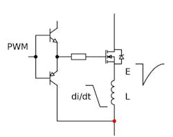
An example is driving the gate of a MOSFET switching at high frequency. The source connection to the device is a common point for the gate-drive voltage and drain-source current. If there’s a common connection inductance, L (Fig. 1), changes in current affect the gate voltage proportional to the inductance and the rate of change of current (Faraday’s Law). When the gate is driven off, a negative-going transient on the source works to offset the negative drive.
1. Source inductance can cause gate voltage transients.
L can be the inductance of the internal source lead of the MOSFET of around 1 nH per mm; if the device is leaded, such as the TO-247 package, the external connections add to L as well. When switching times were measured in microseconds, amps of switched current only produced millivolts of transient, which hardly affected the gate-drive voltage.
Modern wide bandgap (WBG) devices, however, can now switch tens of amps in a few nanoseconds, producing around 5 V per nH of connection inductance. If this adds to the gate drive, there’s guaranteed mayhem. What’s likely to happen is that the voltage opposes MOSFET switch-off, risking at least ringing and at worst shoot-through and device failure.
The effect can be minimized with Si MOSFETs if the gate is driven to a negative voltage when off, sometimes as much as −10 V to defeat the de-bias caused by the voltage spike. This does cause significantly more gate-drive power dissipation, though, which scales with the total gate-drive voltage swing. It’s more of a problem with WBG devices such as SiC and GaN, which can have maximum recommended negative drives voltages of only −3 V or so.
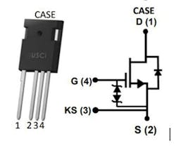
The solution is to “make the Kelvin connection” and ensure that the gate-drive return is as close as possible to the MOSFET die source connection. Although this is easy with chip-scale packaging, if the TO-247 type is preferred for its heat-dissipation performance, the connection has to be a fourth package lead (Fig. 2).
2. Four-lead TO-247 package with source “Kelvin connection.”
Taking the Brakes Off
Switching speeds can now reach the potential of WBG without fear of disturbing the gate drive, to the extent that no negative gate voltage is needed, making the drive circuit simpler and lower cost. When implemented on SiC JFET cascodes developed by UnitedSiC, the effect is dramatic: With equivalent three-terminal packages, the device is internally slowed for reliable operation, but with the four-terminal Kelvin connection type, the brakes are off and current slew rates can exceed 5000 A/µs with clean gate-drive signals. Consequently, devices are capable of operating at higher frequencies with higher efficiency, even in hard-switched applications.
However, there are some things to consider. For instance, the device lead connection inductance still exists in the TO-247 package, and a small snubber may be necessary across drain-source to stop voltage overshoots in the power path. Also, the gate drive loop must still follow good layout practice. It should be as compact as possible for minimum inductance—gate-drive peak currents can be amps, with the same slew rate as the channel current, producing voltage transients across the loop inductance in the gate-drive circuit. A small loop also helps to prevent pick-up from external magnetic fields.
Which Kelvin Connection?
A practical problem can occur when the gate-drive return is connected to the main system 0 V, which is tied to the power ground at some point. It’s probably inconvenient to make this common point the switch Kelvin connection, and if the power circuit is a bridge, there are at least two low-side devices with two Kelvin connections. So which one is connected to system 0 V?
The problem is worse if resistive current sensing is used in the device source lead. If the Kelvin connection is the system 0 V, the voltage generated across the resistor is negative. Again, this is inconvenient at the very least.
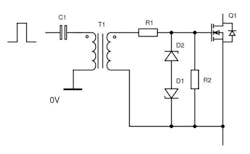
A common solution is to isolate the gate drive through an optocoupler or transformer. This will be necessary for any “high-side” drives anyway, so if included for the “low” side, the Kelvin connection can be “floating,” isolated from system 0 V (Fig. 3). A transformer also gives the option to simply generate a negative off-state gate drive, if desired, and a positive drive scaled to be the optimum value, through the turns ratio. In many practical circuits, the gate drives need isolation for safety if the control electronics is accessible and the power stage is at high voltages.
3. Isolated transformer gate drive.
Kelvin connections for the gates of leaded WBG devices unlocks the use of high-dissipation packages such as the TO-247, bringing us closer to the switch that’s ideal electrically and can be practically used at high power levels. We can thank Lord Kelvin for his contribution, but he didn’t get everything right: In 1902, he stated, “No balloon and no airplane will be ever be practically successful.” Ironically, his eponymous connection in electronics and modern aircraft helps to keep them flying.
Anup Bhalla is VP of Engineering at UnitedSiC.
Reference
https://en.wikipedia.org/wiki/William_Thomson,_1st_Baron_Kelvin


