Download this article in PDF format.
This converter utilizes a resonant capacitor in series with the primary winding. All power must be transferred from input to output by current passing through capacitor Cr. Capacitor Cr’s voltage rating is approximately 1V and yet it converts input voltage of 50V. Therefore, its voltage rating is 50 times lower than the input source voltage. In addition, the required capacitor value is in the order of 100µF, so a very small size capacitor is needed for this 100W, 1V @ 100A converter.
Furthermore, if a 5:1 step down is used to convert to 0.5V, the capacitor needs to handle 5 times reduced rms current of 20A instead of 100A. Likewise, the voltage scaling of the transformer leads to 5 times reduced voltage stresses of the output diode. This, in turn, significantly reduces diode conduction losses when a synchronous rectifier is used.
Operation of this converter can be best understood when the models of the two circuit subintervals are analyzed with the inclusion of the leakage inductance Lr of the Hybrid transformer. Resonant inductance Lr resonates with the resonant capacitance Cr on the primary, resulting in resonant period Tr given by:
Tr = 2π√LrCr (11)
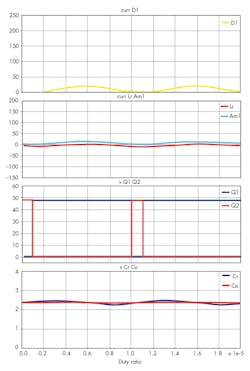
Note that the large magnetizing inductance of the transformer is effectively shorted during the OFF-time interval, leading to a purely sinusoidal AC current on the primary as illustrated in the waveforms in Figures 7 and 8, and the resulting sinusoidal current on secondary. This has crucial consequences for converter operation, as described below.
7. Simulations for 50A DC load.
8. Simulations for 10A DC load.
Leakage Losses Eliminated
When resonant period Tr is equal to the OFF-time interval, the converter achieves a unique optimum operating point given by:
Tr = Toff (12)
Current ip (Fig. 8, again) is continuous at both switching instances, so the losses are eliminated. They normally increase proportionally with increased switching frequency in all other transformer-coupled converters! The bonus is that the primary current is purely sinusoidal with zero average current. Hence, there’s no DC bias contribution from the transformer primary, which substantially reduces energy storage in the transformer. Obviously, there’s a strong incentive for keeping this ideal operating point for all input voltages and load current conditions.
Optimum Control Method
We can preserve the ideal operating point given by Equation 12 by simply keeping the OFF period (Toff) constant. Clearly, the variation of the ON-time period will then provide direct output DC voltage control. Obviously, this calls for variable switching frequency control. Nevertheless, for large step-down voltages resulting from low duty ratios, such as D = 0.1, this effectively results in a near constant switching frequency with only about 10% frequency variation. Optimum control is then:
Toff = Constant (13)
The DC voltage conversion follows the rectangular voltage excitation of the hybrid transformer as used for derivation of the voltage conversion. Hybrid transformer currents, however, are sinusoidal, also satisfying the turns ratio of the hybrid transformer.
The yellow waveform in Figures 7 and 8 show the diode current clearly confirms that the diode is both turning ON and turning OFF at ZERO current; hence, no switching losses. In fact, as its voltage at both switching instances is also ZERO, the diode doesn’t even know that it’s switching! Practical consequence: no spikes and no EMI generated.
Obviously, the proper drive for active switches operating with zero voltage switching (ZVS) eliminate switching losses of active devices, as well as spikes and EMI noise typically associated with them. The bottom line is that all switching and leakage losses are eliminated, leaving only resistive losses. Therefore, the efficiency is over 99% and EMI is low.
Simulations demonstrated that diode current always operates in continuous conduction mode (CCM) for all loads. As expected, there’s also no change in the voltage-conversion gain as seen in all simulation waveforms. Furthermore, the high efficiency at full load is also maintained at very light load, as there are no large circulating currents present in a synchronous buck converter at light load.
Sinusoidal Waveforms
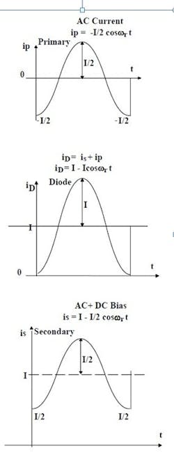
Figure 9 shows the three-key sinusoidal-like waveforms for the special case of 1:1 transformer turns ratio, which were analytically derived earlier. This is made to better understand the fundamental principles. The general case for N1 to N2 turns ratio can then be easily derived and equations generalized using the usual transformer current scaling law via its primary to secondary turns ratio.
9. Sinusoidal-like waveforms for the special case of 1:1 transformer turns ratio: Primary ip = AC current (top); diode current iD = is+ip (middle); and secondary current is = AC+DC bias (bottom).
Synchronous Rectifier MOSFET Implementation
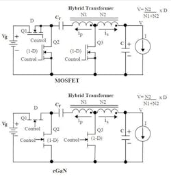
Of the remaining conduction losses, by far the largest loss contribution for low output voltages, like 1V, are due to conduction losses of the rectifier Cr diode. This can be mitigated by using a MOSFET with ultra-low on resistance, such as in Figure 10. It’s important to note the distinction between operation of this MOSFET in the Hybrid Switching converter and the synchronous buck converter with MOSFET.
10. MOSFET and GaN implementation.
In the buck converter synchronous rectifier, the MOSFET must be a current bidirectional switch to enable current flow through that MOSFET for light-load to no-load conditions. In the Hybrid Switching converter, the sync MOSFET Q3 always bypasses diode current conduction at any load, including no load. In fact, instead of a MOSFET, one could use a diode implemented with GaN technology, thus eliminating the need for control!
An All-GaN-Transistor Implementation
An ideal implementation of this switch would be to use a dual-gate GaN device, such as the recently introduced Panasonic devices that emulate the diode conduction without having the limitations of the body diode of MOSFETs. This, in fact, lends itself to a new power integrated-circuit (PIC) implementation.
The GaN switching devices have a unique property that all GaN power devices in Fig. 10 can be built on a same die. This eliminates the very lossy and space-wasting connection for making connections between separately packaged discrete devices. Moreover, the high-side drive circuit and the direct drive for synchronous GaN device can all be built on the same substrate, making it a single Power and Drive Chip.
The bonus from operating GaN devices at 100kHz switching frequency isn’t only that gate-drive losses are practically eliminated, but also the fact that paralleling several devices does decrease conduction losses greatly without increasing gate drive losses, as would be the case for MOSFET implementations.
Is Feedback Needed to Regulate the Hybrid Switching Converter?
No! The reason feedback is always used in conventional converters is because:
- Low efficiency in the 80% and low 90% range requires a change of duty ratio to compensate for the drop of the voltage caused by large differences in converter losses between full load and about 20% load.
- All present converters with diode rectification result in discontinuous inductor mode at no load to light load and need a substantial change in duty ratio to maintain voltage regulation.
- Change of input voltage also requires a change of duty ratio to keep output voltage constant despite input voltage changes.
In the Hybrid Switch converter, the third bulleted item above can be solved using classical feedforward control by varying the PWM sawtooth ramp magnitude with input voltage. Hence, voltage changes are compensated quickly within a single switching cycle. The Hybrid Switch converter solves the first two items by having ultra-high efficiency and no DCM operation.
With efficiencies of 99% and above, no feedback control regulation is needed. Not only is it not needed, but it’s also not desired due to a couple of drawbacks caused by feedback:
- Oscillation and stability problems can result in potential catastrophic failures.
- Grossly limiting bandwidth to 10% or so of the fundamental open-loop bandwidth can result in diminished transient response.
The remaining issue is how to change output voltage to the discrete levels demanded by microprocessors. This can also be handled by controlling the PWM sawtooth ramp, using a separate reference analog voltage to control the output DC voltage continuously; not just in discrete steps.
Videos of Simulations for Full and Half Loads
A video simulation was made at a 15A load, which confirms continuity of the primary current exhibiting no current jumps as well as the diode turning on and off at zero current.
NOTE: This converter is protected by a US Patent applied on March 28, 2011 and issued on January 6, 2016 as US 9,231,471 B2.
Companies interested in licensing the converter and partnering with TESLAco to develop products are welcome to contact Dr. Slobodan Cuk at [email protected] or via Skype on slobodan.cuk.
ANNOUNCEMENT: 2nd MASTERCLASS - March 25-28, 2019 during Spring-break at UC Irvine following March 17-21, 2019 APEC conference in Anaheim (approx. 10 miles from UC Irvine)
The 2nd Masterclass will be a 4-day event divided as: CLASSIC POWER ELECTRONICS (first two days) and NEW POWER ELECTRONICS (following two days). The course will include detailed explanations of this Hybrid Switching converter and a number of others along with their simulations verifications using live demonstrations with .plecs and SIMPLIS simulation software.
Highlights of the 1st masterclass on Sept.25-27, 2018 can be found at https://goo.gl/7LMmWG.
To register, visit https://teslaco.com/courses.


