Download this article in PDF format.
When you connect the gate to the source of a JFET (junction field-effect transistor), it becomes a two-terminal current source. The current that will flow is called IDSS (current, drain-to-source, saturated). One problem you might face is that the IDSS of FETs is quite variable for different parts of the same number. The size of the JFET will determine the rough range of the current, but it does change over temperature. JFETs are depletion-mode devices that conduct until you apply a negative voltage to the gate relative to the source.
Still, having an inexpensive two-terminal current source can be quite handy. If you connect a source-connected JFET to a Zener diode, you will improve the voltage regulation of the diode, since it’s now stabilized at a fixed current no matter the input voltage to the network. This arrangement might be less expensive than an IC regulator. It also may be slightly more reliable, since the circuit is just two components that are quite reliable to begin with. Undersea fiber optic cables use power supplies that are just a large Zener diode.
A single component and a dropping resistor or JFET is about as simple, and hence, about as reliable as you can get. Sure, there’s a lot of waste heat, but dissipating heat at the bottom of the ocean is not a problem, whereas a power-supply failure down there is a big problem.
It’s in the Curves
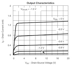
The constant-current nature of a JFET is a function of its characteristic curves (Fig. 1). The current through the device tends to level out once the voltage gets high enough. The IDSS current is when VGS, the voltage between the gate and source pins, is 0 V. The topmost curve in Figure 1 shows that condition. The deviation from a constant-current source is represented by the small slope and bow of that curve. As the gate-source voltage becomes more negative, the constant current reduces. However, the slope of the curve also flattens out, better approaching a perfect source.
1. The JFET characteristic curves show the through current being relatively constant over changes in applied voltage. (Courtesy of Vishay)
One problem with JFETs is that they vary from part to part. The datasheet that Figure 1 came from has a similar chart for when VGS(off) = −0.7 V. This tells you that the parts may have a pinch-off voltage anywhere between −0.7 and −1.5 V, the voltage condition of the chart in Figure 1. JFETs have a lot of part-to-part variation because their transistor action is controlled by the diffusion of the silicon as well as the lithography.
It’s easy to make repeatable parts with lithography; accuracy is assured with modern machinery that gets line widths well below 50 nm. That’s why transistor density is so high in digital chips. Diffusion is not controlled by a precise mask, but by time and temperature in a diffusion furnace. This is a less accurate process, and that’s why JFETs have wider tolerances than conventional transistors. While a given part number may have a variation of IDSS over its production, you can hand-select the parts to tighten up the current tolerance. There are testing services that will do this for you, and some JFET manufacturers might do this for you.
Noise and Speed
JFET current sources tend to have low noise. This is because a JFET is a buried device on an IC die. Since the junction is not working at the surface of the part, there are fewer crystal defects and impurities that cause noise. So, a JFET may be a way to make a low-noise current source or voltage regulator. The simplicity of the circuit also means it will respond with low latency to input voltage changes. This transient response might be an essential spec for your current source. The transient response is based on the physics of the junction, not just hanging a big capacitor on a voltage regulator.
Finding the Optimum Circuit
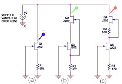
There’s an old application note about using JFETs as a constant-current source. That article says you can achieve better regulation by putting a resistor in the source leg of the circuit (Fig. 2a). This makes the JFET operate on one of the lower curves in Figure 1. The app note goes on to show that a cascode of two JFETs will have even better performance (Fig. 2b). I did Spice simulation of these circuits, and tried just two current sources in series (Fig. 2c).
2. Three approaches to a JFET current source: The simple circuit, with a source resistor chosen to reduce the temperature coefficient of the circuit (a); a cascode circuit that gives tighter performance (b); and a series circuit (c) that has better regulation than (a) but less temperature coefficient than (b), if you believe PSpice.
Bob Pease used to say “Spice lies!” and I am beginning to see why. Using my old OrCAD PSpice 9.2, I tried to replicate the circuit using the same 2N4339 JFET shown in the curves of Figure 7 in the app note. The problem was the Spice model for the 2N4339 in PSpice was nowhere close to the curves in the app note. On a hunch, I then tried the J202 JFET, which is supposed to be the plastic package equivalent to the metal-can 2N4339. That PSpice model was different by a factor of four. Since it was closer to the app note figure, I used that model.
After a lot of grief, which I will detail below, I came up with the simulation results (Fig. 3). The simple circuit (blue) has the highest deviation. The cascode circuit (green) is much flatter. It has almost the same compliance as the single-transistor circuit; that is, it will work close to 0 V. Unfortunately, the spread of the three green curves show how sensitive the cascode is to a wide temperature swing, between −55 and 125°C. The response of the series circuit of Figure 2c (red) is twice as flat as the simple single-transistor circuit, and it has less variation over temperature than the cascode.
3. Shown are PSpice results of the circuits in Figure 2 for −55°C, 25°C, and 125°C. The simple circuit in blue has the most change over applied voltage. The green traces of the cascode circuit are flatter, but the 25°C trace is the lowest one—a significant outlier. The red traces are a series circuit that’s flatter than the simple circuit, but less variation over temperature than the cascode circuit. The 25°C trace for the red and blue circuits are in the middle of the group, not an outlier like the cascode circuit.
Spice Might Lie
Of course, all this could just be Spice lying to us. Yet Spice rarely lies on a single-transistor circuit. What Spice does is remind us that there may be temperature coefficient problems that arise with different parts and different bias values. The app note implied a good bias voltage was −0.83 V, with a source resistance of 5 kΩ. I found a bias voltage of −0.6 V was closer to a low TC, but there was no voltage what would work at −55°C and +125°C. My source resistor ended up at 570 Ω.
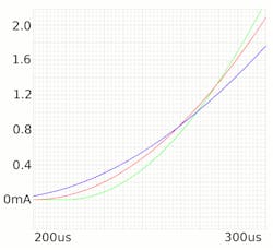
The Figure 7 in the app note showed a VGS voltage where the current source would have zero temperature coefficient. The Spice model did not agree with this assessment. To figure out what was going on in the Spice model, I did a three-temperature run of a J202 JFET with 10-V drain-source and a sine-wave source on the gate, with an amplitude of 8 V and an offset of −4 V. By doing a 1-ms transient sweep, and setting the sine wave generator to 250 Hz, this means the gate voltage will go from −4 V to 0 V on the simulation output.
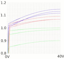
If the transfer characteristic in Figure 7 of the app note was correct, there should be a gate-source voltage where all three curves converge. This was not the case in my PSpice simulation (Fig. 4). But it does show the curve at 25°C (red) will cross the low and high temperatures at two points. This means you can set up a source resistor to create a gate bias that will have no TC between room temperature and 125°C (blue) or room temperature and −55°C (green), but not both.
4. A J202 JFET Spice model shows current at three temperatures as the gate voltage increases. According to Spice, there’s no place where all three traces cross. Instead, you can establish a gate bias voltage to eliminate the TC between 25°C and 125°C, or 25°C and −55°C, but not both.
A Two-Terminal Current Source
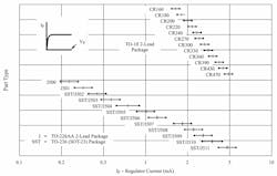
In addition to using JFETs as a current source, there are two-terminal current source diodes available (Fig. 5). These are JFETs with the source connected internally. They tend to be expensive, but the specs assure you have a known range of IDSS, so it may be worth it to you. These parts have been available for decades, so there should not be any sourcing problems in production.
5. The Siliconix line of two-terminal current diodes are obsolete from them, but available from Linear Systems. (Courtesy of Vishay)
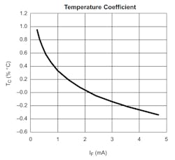
While there are no TC curves of a given part, the Vishay datasheet does have a TC versus current chart (Fig. 6). I interpret this as meaning a 2-mA part, such as CR200 or SST/J510, would have close to no tempco. It gets pretty scary for currents at the extremes of the chart—the axis is not PPM, but rather, percent change per °C. That means a 500-uA part would change value by 50% with 100°C of temperature change.
6. The temperature coefficient of the two-terminal current diodes is low for 2-mA parts, but gets pretty horrific for parts at the extremes of the current range. (Courtesy of Vishay)
Simple and Reliable
Bob Pease has written extensively on current sources, including the Howland current source. Once you commit to using an op amp, you can get remarkable precision and decent cost. Still, you should keep the simple JFET or current-regulating diode in mind. And note the “CR” prefix for diodes in old schematics come from “current-regulator.” Sometimes old circuits are the best circuits, as long as they get the job done, over the temperatures you need them to work.
