While attending APEC 2019, it seemed that gallium-nitride (GaN) transistors were just coming into their own in high-volume applications, while silicon-carbide (SiC) transistors have found wide applications in the here-and-now. GaN transistors, and the parts and printed-circuit-board (PCB) design you need to support them, are still fairly expensive. For space applications, which need radiation hardness (rad-hard), GaN makes sense, as does some industrial applications. Where you rarely see GaN in 2019 is in high-volume, low-cost consumer devices.
A semiconductor company executive challenged me to take apart any consumer charger or other low-cost device and find a GaN transistor. Turns out there are some low-cost chargers available that use GaN transistors. So, it looks like GaN has broken into the mainstream. The executive also acknowledged that SiC transistors and diodes are going mainstream even today.
SiC transistors are suitable for fast-switching, high-voltage power supplies. While high-voltage power is not needed in consumer electronics, it’s used in solar-panel inverters, electric cars, and perhaps a dc charger in your Tesla Powerwall battery storage system. SiC is already used in more expensive industrial systems, like servo drives, welders, uninterruptible power supplies (UPS), commercial electric vehicles, and medical systems.
A New SiC Driver Chip
Michael Hornkamp, senior director of marketing for gate-driver products at Power Integrations notes, “Silicon-carbide MOSFET technology opens the door for decreasing size and weight as well as reduced losses in power inverter systems.” Acknowledging the great potential of SiC widespread adoption, Power Integrations has introduced a single-channel isolated SiC gate-driver chip, the SIC1182K (Fig. 1). The parts cost $4.65 in 10,000-piece quantities.
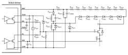
1. The SIC1182 SiC gate driver chip is fully isolated. The VTOT symbol represents an external isolated 15-V supply that you provide to the IC. The squiggles between the resistors and diodes indicate there are more of them stacked to get your required voltage standoff rating.
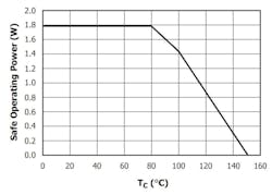
To get a SiC transistor to switch fast, you need a sizable drive current to charge and discharge the gate capacitance. The SIC1182K sources and sinks 8 A even at 125°C. This means you can design dc-ac inverter circuits that handle several hundred kilowatts of power. Switching speed of the driver IC can be as has high as 150 kHz. Note that you must derate the power that the IC can supply over temperature (Fig. 2). The faster you switch the chip and the bigger the SiC transistor gate capacitance you have, the more power the SIC1182K will dissipate.
2. You have to derate the power delivered by the SIC1182K when it operates at high temperatures. Realize the chip self-heats, so you must look at the temperature rise it generates in addition to the maximum ambient temperature.
To achieve the isolation rating, Power Integrations leverages its trademarked FluxLink technology. This uses the leadframe and bonding wires inside the IC as magnetic coupling coils. This does away with slow optocouplers that are subject to long-term degradation. It negates the need for capacitive or silicon-based isolators, which the company claims significantly improves reliability.
Power Integrations also claims the 1200-V isolation in the IC exhibits good immunity from external magnetic fields. I knew an engineer that debugged a burn-in rack control system. He was supplying hundreds of amperes of dc current to the devices undergoing burn-in. The rack vendor had looped the cables inside the rack in such a way that the magnetic fields generated by the dc currents were so strong they would pull in the control relays. You will have to deal with magnetic fields in any high-power application, so be aware.
In addition to magnetic-field immunity, the SIC1182K provides protection features such as current-sense readout, desaturation monitoring, and advanced active clamping. The part offers undervoltage lockout (UVLO) on both the primary and secondary power supplies. The shutdown circuits operate within five microseconds.
Watch Your Creepage and Clearance
High-voltage circuits need to provide a clearance distance between the high-voltage wires. A greater distance, called creepage distance, is required when the voltage has a surface to run across, such as a circuit board or IC plastic package. The SIC1182K package has over 9.5-mm creepage and clearance distance. The case uses a material with the highest comparative tracking index rating (CTI), CTI600 to the IEC60112 international standard.
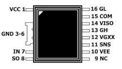
The pinout of the IC allows you to use a two-layer PCB (Fig. 3). While this is good for a cost reduction, you might want to design the PCB in four layers for the prototype. It’s always good to have a ground plane and fewer vias. Some designers flip the layers around before production to put the signal layers on the inside and power and ground on the outside. This turns the PCB into a Gaussian chamber that shields the signal wires and prevents electromagnetic interference (EMI) from radiating out of the traces.
3. The designers of the SIC1182K made sure to provide for adequate creepage and clearance distances, as well as making a pinout that simplifies your board layout.
You have to worry about EMI on any fast circuit; SiC circuits are not only fast, they tend to be high current. The di/dt, the rate of change of currents, is what causes radiation and spikes and other problems. Make sure the PCB layout and supply wires are short and have small loop areas. Even thick copper bus bars will have an inductance that can cause over- and under-shoot problems that might blow up your power devices.
Look Out for Spikes
To see those fast transients, make sure you have a fast oscilloscope to monitor the signals. A 100-MHz ’scope is not always adequate. A 400-MHz scope is preferable, and fast digital scopes are OK if you understand the bandwidth and sampling speed settings that will allow you to see ringing or other problems on the gate.
I worked on a high-voltage power supply for traveling wave tubes (TWTs) on a radar jamming pod for fighter aircraft. The design used stacked MOSFETs to get the voltage output. The technician was perplexed since the transistors kept blowing up “for no reason.” He was using a slow digital scope to monitor the gates. I advised to use a 400-MHz analog scope and he then saw the gates break into oscillation at over 500 MHz. The fix was to equalize the trace length on the gates, and to put in a low-value resistor in the gate drive to damp the oscillations. Problem is, that also slows down the turn-on and turn-off times. So like all analog, it’s a tradeoff.
It’s also advisable to have a FET oscilloscope probe to look at the gate circuits. A regular probe has over 7 pF of capacitance, and at the speed the SIC1182K can provide, that’s a lot of added load to the gate trace. A FET probe gets the probe capacitance down to 2 pF or less, but you still have to realize the probe will affect your circuit.
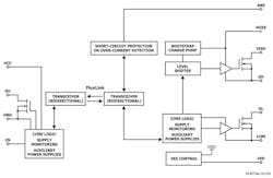
The block diagram of the SIC1182K (Fig. 4) reveals the internal charge pump needed to create a gate-drive voltage above the VISO isolated supply that you must provide to the secondary side. That voltage is brought out on pin VGXX so that you can connect an external ceramic capacitor to store the energy created by the charge pump. The diagram also shows the protection circuits, and the FluxLink isolated coupling scheme.
4. The block diagram of the SIC1182K depicts the internal high-voltage isolation as well as the extensive protection circuits in the IC. The FluxLink isolation comes from using the die bond wires and leadframe to create a magnetic coupling.
A Detailed Schematic
An example circuit shows the secondary-side components you need for a SiC driver (Fig. 5). Note the strings of resistors, RCEX, and diodes, DTVSX, that you need to achieve the voltage standoff rating. With a high-voltage circuit, you choose the physical size of the resistors not only for the power they dissipate, but for the voltage rating they provide. A 1206 size has much better voltage rating than a 0805. The same goes for the diodes used for snubbing—make sure the stack you use has an adequate voltage rating.
5. There are many secondary components you provide to drive a SiC transistor. This shows the separate resistors and diodes omitted on Figure 1.
Another thing to note in the circuit is the small voltage source symbol VTOT. Be aware that represents an entire 15-V isolated power supply that you must create to feed the chip’s secondary circuits. This power supply needs to have an isolation rating at least as good as the SIC1182K, which is IEC60664-1 for equipment below 1000 V and IEC61800-5-1 electric motor drives. Power Integrations is working on getting UL 1577 with 5 kVac for 1 minute, as well as VDE0884-10. You should make sure the external isolated 15-V supply has good transient response for the fast high currents that the IC will demand. Be sure to put decoupling capacitor CS2 near the IC to provide the least amount of ground bounce and ringing.
The SIC1182K is available now and comes in tubes of 48 pieces (no suffix) or in 1000-piece tape-and-reel (TL suffix). If you have not designed high-speed, high-current analog circuits, you would be advised to talk to Power Integrations’ application engineering department, who will make sure you have an appropriate design for the part. They want you to succeed in the design as much as you and your boss do.


