A New “Star” Emerges for High-Density DC-DC Converters
Toshiba unveiled a new power switching topology that could usher in more compact, more efficient DC-DC converters. These devices would be able to handle the huge amounts of current required by AI silicon and other next-gen chips.
The company said its “star-delta switching topology” converts power with up to 88% efficiency and delivers high current densities of up to 790 mA per mm2. The non-isolated DC-DC power topology uses a combination of capacitors and inductors to step down a 48-V input to a 1-V output, which saves space by eliminating the need for bulky transformers. Higher efficiency helps to reduce heat before it saps the server or other systems’ performance.
According to Toshiba, the 48-V-to-1-V DC-DC converters based on the new topology could be used in everything from 5G base stations to data centers. They could also apply to 48-V automotive power systems, which are becoming more prevalent as new power-hungry subsystems under the hood overload the traditional 12-V bus.
While it’s still testing out the new power switching topology, Toshiba plans to implement it in future DC-DC converters.
Solving the “Last Inch” of the Power Delivery Problem in AI
Modern systems-on-chips (SoCs) consistently require more and more power, and they show no signs of slowing down.
In data centers, the latest graphics processing units (GPUs) and other AI chips, led by NVIDIA’s Hopper GPU and future Blackwell GPU that burns through more than 1 kW, are driving up the demand. The power used by even a single column of servers is skyrocketing to more than 90 kW, up from 15 to 30 kW. After electricity enters the data center from the grid, but before it enters a processor, it runs through a power-supply unit (PSU) that steps down the AC mains voltage to a smaller DC voltage that can be handled by the server.
But once it enters the server, it becomes much more difficult to deliver all of that power over the motherboard and into the point-of-load (PoL)—the so-called “last inch” of the power-delivery network (PDN)—so that the processor runs to the best of its ability under dynamic loading conditions. Toshiba and other industry leaders are going all out to develop DC-DC converter ICs that can deliver the appropriate power smoothly and efficiently.
The focus is on the voltage regulator module (VRM)—a type of DC-DC converter that steps down the 12-V DC voltage output by the PSU so that it can run the processors and accelerators inside the server, which in many cases operate with voltages of less than 1 V. As modern chips consume more power, DC-DC converters in front of them must handle incrementally larger load currents, which are hitting more than 1000 A in the most advanced AI accelerators. Incidentally, high currents increase conduction losses in the interconnects between them, noted Toshiba.
To curtail these losses, the technology industry is upping the DC voltage used to ferry power into and inside servers to 48 V. For decades, the standard DC bus voltage employed in data centers was 12 V. Upgrading to 48 V reduces the required current by a factor of four since Ohm’s Law states that power is equal to current times voltage (P = I × V). Since power also equals the resistance times current squared (P = R × I2), adopting a 48-V bus voltage reduces the losses caused by resistance on the power rails by 16X.
A New Switching Topology for a New Age of Power Delivery
Minimizing power losses in data centers is all about distributing power at higher voltages and lesser currents, then stepping down the voltage as close as possible to the “core” voltage of the processor. Toshiba and other players in the power semiconductor industry are racing to roll out compact and cost-effective DC-DC converters that can step down 48 V to 1 V very efficiently—so efficiently that you can cut out any secondary steps between them.
But that’s not so easy. In the case of the buck topology, managing 48 V instead of 12 V means the width of the pulses—the pulse-width-modulation (PWM) signals—driving the power switches at the heart of the DC-DC converter must be 4X shorter, said Toshiba.
PWM works by rapidly changing the width of digital signals to produce the desired analog signal to control the operation of the power switch. It gives you the ability to regulate the average output current and voltage that a power supply delivers to a load.
Reducing the width of the PWM signals increases the DC-DC converter’s duty cycle. The tradeoff is the switching speeds required to do so are significantly faster than usual, Toshiba said.
Therefore, while the 48-V DC bus reduces conduction losses, the faster switching required to use it inevitably causes DC-DC converters based on the buck topology to suffer higher switching losses. That cancels out the power efficiency gains, said Toshiba.
In most cases, you can use transformers in isolated power topologies to take care of the duty expansion. But these components require a relatively large amount of space that can add up in multiphase DC-DC converters, which are widely used to deliver power to AI chips and other high-current loads with very fast response times. The switched-capacitor topology throws out the transformers to save space in the system, but it comes with other drawbacks.
The other possibility is to use “hybrid” power topologies that leverage a combination of inductors and capacitors instead of transformers. These non-isolated DC-DC converters can occupy 10X to 100X less space in a system, said Toshiba. The tradeoff is that they must be paired with many more high-frequency capacitors to increase the duty cycle of the PWM, leading to more congested pin wiring. More components also equal higher costs.
Toshiba's Star-Delta Topology: A New “Star” in DC-DC Converters?
Toshiba is trying to solve these shortcomings with its star-delta switching topology for non-isolated DC-DC converters, which was recently presented at the annual IEEE Symposium on VLSI Technology and Circuits.
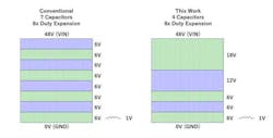
The new topology merges the switching layers on the front end of the DC-DC converter, where the current is comparably small, reducing the total capacitors required by close to half. In DC-DC converters, switching “layers” are divisions formed by the switching of intermediate nodes.
In a standard hybrid power topology, there are eight equally divided switching layers that step down the 48-V voltage at the input 6 V at a time. The buck topology, on the other hand, requires a single switching layer with the switching amplitude of the input voltage.
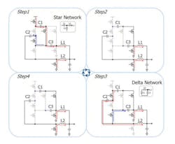
When power is turned on, the DC-DC converter runs through steps one to four in the switching process, with the capacitors configured in a “star” network—the name derived from the wiring being arranged in the shape of a star—for the first step and then in a “delta” network—with the wiring arranged in a triangle—for step three. Every single switching layer runs through all four steps at once. As Toshiba explained, the new topology switches through all four steps repeatedly to generate all of the switching layers at the same time.
While every switching layer in the star-delta topology uses a minimum of one capacitor, Toshiba said it reduces the number of capacitors by optimizing the number of switching layers in the first place. Merging these switching layers requires the use of high-voltage switches that are unnecessary in other non-isolated power topologies. But since the current is minimal, the power FETs themselves are smaller.
Toshiba plugged the new power switching topology into a 48-V-to-1-V DC-DC converter. With fully integrated power switches, the test chip can deliver high current densities of 730 to 790 mA per mm2 while bringing 80% efficiency and 2.5-MHz frequency to the table. Toshiba said it also developed a bootstrap circuit with extra-low capacitance to enhance the power efficiency and reduce the total layout area by more than 60%.
To cut down on power dissipation, Toshiba developed a level-shifter circuit that features an active bias current scheme. It reduces bias current by up to 92% and contributes to a conversion efficiency of up to 88%.
A level shifter is used to adjust the voltage level of an input signal with the same waveform. Most DC-DC converters require a level shifter for each of its power switches. The reason is that the power devices are configured in a stack connection and the reference voltage value of each switch can vary.
Toshiba explained that its level shifter is designed to cancel out the switching noise of the bias current before it leads to failures. As a result, the level shifter reduces bias current in the idle state.
Since many of the most advanced chips on the market run on supply voltages of less than 1 V, Toshiba said the DC-DC converter can use dynamic voltage and frequency scaling (DVFS) to step down to 0.3 V.


