This Week in PowerBites: Protection Devices, Ref Designs, and the World's Gnarliest eBike
This article is part of the This Week in PowerBites Library Series.
What you’ll learn:
- New generations of smarter devices provide enhanced protection against overvoltage and overcurrent conditions.
- Reference designs are simplifying the development of many charging applications ranging from EV charging stations to high-powered USB-C supplies.
- How hybrid-electric propulsion is accelerating the transition to electric aviation.
- Is the world's gnarliest on-/off-road eBike really worth $7,500?
The process of electrifying the world's fleet of cargo and passenger aircraft appears to have begun. It will most likely occur in a series of evolutionary phases, each lasting multiple decades. During this transitional period, hybrid-electric propulsion systems could dramatically cut aircraft CO2 emissions and operating costs while serving as a "technology bridge" to the development of practical all-electric aviation.
To see if hybrids really have "The Wright Stuff," check out "An Introduction to Hybrid-Electric Aircraft (Part 1).” In this first installment of Electronic Design's exclusive three-part series, you'll learn about the advantages of electric aviation, the limitations of today's battery technologies, and how hybrid-electric propulsion systems can overcome them.
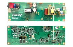
Pulsiv Limited announced the release of what it claims to be the world’s most efficient* 65-W USB-C gallium-nitride (GaN)-optimized reference design. Developed to address the complex challenges associated with thermal performance in power supplies, the PSV-RDAD-65USB reference design combines Pulsiv OSMIUM technology with an industry-standard QR flyback architecture, a half-active bridge, and highly optimized, ultra-compact magnetics. It achieves 96% efficiency while running 30% cooler than other comparable designs.
The OSMIUM reference design demonstrates a significant improvement in thermal performance and reduces critical component temperatures by more than 30% compared to other designs. At full load, the flyback transformer reaches 33.9°C at 230 V AC and 30.3°C at 265 V above an ambient temperature of 26.1°C.
This achievement is likely to set a new benchmark and enables 65-W fast charging in space-constrained environments and/or heat-sensitive applications such as in-wall plug sockets that incorporate USB-C connectivity.
Unique Features Deliver High Efficiency
The OSMIUM controller technology senses AC line voltage and frequency to adjust capacitor charging time, preventing the circuit from drawing any line current at the AC zero voltage crossing. MOSFETs in the lower half of the AC-to-DC bridge are carefully controlled, in combination with high-side diodes. The half-active bridge in this design strikes the delicate balance between efficiency, cost, and complexity, and it supports universal input with efficiency gains of 0.7% at full load from a 115-V AC supply.
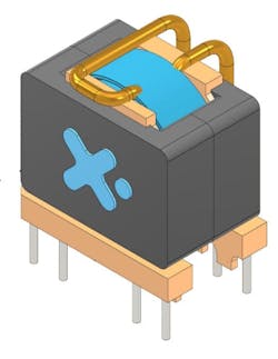
This enables the controller to generate a HVDC output that varies between the peak AC input and 150 V to drive the QR flyback at maximum efficiency. The wider voltage range significantly reduces primary-side inductance to enable the use of an EQ20 transformer, which was developed in partnership with magnetics experts Frenetic. Together, these features result in a 20% size reduction and 50% efficiency improvement compared to an RM8 core typically used in other designs.
In addition, GaN transistors from Innoscience have lowered the RDS(on) and parasitic capacitance to reduce losses and optimize cost in both the flyback and synchronous rectifier subsystems.
*Efficiency based on peak thermal measurements at full load after 30 mins.
Design Package and Eval Boards Available
The PSV-RDAD-65USB document package is available for download from the Pulsiv website and includes a datasheet, schematics, bill of materials, and Altium files. The PSV-EBAD-65USB evaluation board enables rapid lab testing and can be pre-ordered now for delivery in the second half of August through a network of franchised distribution partners.
Two new families of advanced surge protective devices (SPDs) from Bourns Inc. are able to deliver high levels of overcurrent and overvoltage protection for AC and DC applications. Both model series have a replaceable modular design and include a window fault indicator and remote alarm, providing enhanced surge-protector operating status monitoring.
AC SPDs
Bourns’ new Model 1270 and 1280 series DIN-rail AC SPDs are IEC/EN 61643-11-compliant Class I + Class II/T1+T2 SPDs. Model 1280 features an advanced Thermal Disconnector (TD+) for enhanced protection that eliminates the need for upstream overcurrent protection. Offering superior surge protection, they deliver up to 80-kA, 8/20-µs per mode surge energy capability, have a high short-circuit current rating up to 50 kA RMS, and an impulse current capacity up to 12.5 kA 10/350 μs.
For detailed product information, go here.
DC SPDs
Bourns Model 1430 and 1440 Series DIN-rail DC SPDs are IEC/EN 61643-31-compliant for Class I + Class II/T1+T2 applications. Designed to protect DC power systems, the 14 new models offer protection voltage ranging from 48 up to 1,500 V DC and feature high-energy MOV technology. In addition, the Model 1440 Series integrates an advanced TD+ to deliver an elevated level of protection that helps eliminate the need for upstream overcurrent protection. Offering superior surge protection, they deliver up to 80-kA 8/20-μs per mode surge energy capability and provide an impulse current capacity up to 12.5 kA 10/350 μs.
For detailed product information, go here.
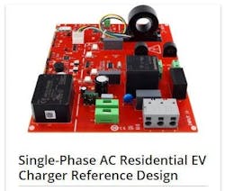
Microchip Technology's family of three flexible and scalable EV charger reference designs can help developers accelerate their time-to-market of an EV charger while meeting the unique requirements of a particular market. At present, the series includes complete designs for a single-phase AC residential system and two three-phase AC commercial systems, each capable of supporting the Open Charge Point Protocol (OCPP).
All three reference designs were developed to be robust, weather-resistant, and user-friendly products that minimize both BOM and manufacturing costs. In addition, they enable manufacturers to meet target markets with a range of scalable solutions that can be tailored to meet specific regional requirements. They include complete hardware design files and source code with software stacks that are tested and compliant with relevant industry-standard communication protocols.
Overview
A Single-Phase AC Residential EV Charger offers a cost-effective and convenient solution for home charging, using a single-phase supply. The on-board high-performance energy-metering device with automatic calibration simplifies the production process. The design has integrated safety protection features including Protective Earth Neutral (PEN) fault detection and Residual Current Device (RCD) detection.
A Three-Phase AC Commercial with OCPP and Wi-Fi SoC EV Charger is intended for high-end residential and commercial charging stations. It features OCPP 1.6 stack integration for communication with charging networks and Wi-Fi SoC for remote management.
A Three-Phase AC Commercial with OCPP and Display EV Charger caters to commercial and public charging stations with a focus on robust operation, including a completed architecture review according to UL 2231. It’s designed to support up to 22 kW with bidirectional charging capabilities and a modular architecture. The design also features a robust graphical user interface (GUI) with a thin-film transistor (TFT) screen and touch input designed to withstand harsh environments.
Development Tools
The EV reference designs are supported by the MPLAB X Integrated Development Environment (IDE) to help designers minimize development time, as well as the MPLAB Harmony v3 and MPLAB Code Configurator.
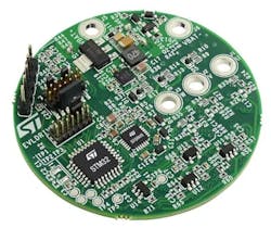
The EVLDRIVE101-HPD (high power density) motor-drive reference design from STMicroelectronics packs a three-phase gate driver, STM32G0 microcontroller, and 750-W power stage on a circular PCB just 50 mm in diameter.
The board features extremely low power consumption in sleep mode—below 1 µA—and its tiny outline can fit directly in equipment like hairdryers, handheld vacuums, power tools, and fans. It also fits easily into drones, robots, and drives for industrial equipment such as pumps and process-automation systems.
Built with ST’s robust and compact STDRIVE101 three-phase gate driver, the reference design gives flexibility to choose the motor-control strategy, such as trapezoidal or field-oriented control (FOC), with sensored or sensorless rotor-position detection.
The STDRIVE101 IC contains three-half bridges with 600-mA source/sink capability and operates from 5.5 to 75 V to handle any low-voltage application. The chip integrates voltage regulation for the high- and low-side gate drivers and configurable drain-source-voltage (VDS) monitoring protection. It also provides an external pin for choosing direct high- and low-side gate inputs or PWM control.
Developers can take advantage of the STM32G0 single-wire debug (SWD) interface to interact with the microcontroller, while support for direct firmware update allows for application of bug fixes and new features.
The power stage of the EVLDRIVE101-HPD reference design features STL220N6F7 60-V STripFET F7 MOSFETs, which preserve efficiency with their 1.2-mΩ typical RDS(on), easing plug-and-play connection of the motor. Additional features include fast-acting power-on circuitry that disconnects the power source when idle to save energy and extend operation in battery-powered applications.
Protection built into the driver IC ensures system safety and efficiency, including the VDS monitoring of the power-stage MOSFETs, as well as undervoltage lockout (UVLO), overtemperature protection, and cross-conduction prevention.
The EVLDRIVE101-HPD is ready to use out of the box and is available now from the eSTore for $92.00.
Nexperia’s NPS3102A and NPS3102B low-ohmic (17 mΩ), high-current (13.5 A), resettable electronic fuses (eFuses) can help protect downstream loads from exposure to excessive voltages. They also protect power supplies from load faults and large inrush currents with 10% current-limiting accuracy.
Both devices have been designed for use in various 12-V hot-swap applications including enterprise communication and storage equipment found in data centers. These include solid-state and hard-disk drives, servers, Ethernet switches, and routers.
The eFuses have a wide input voltage range (21 V abs. max) and an integrated low-resistance pass MOSFET that minimizes voltage drop and power loss. The current clamp limit can be adjusted in the 2- to 13.5-A range using a resistor at the ILIM pin, which can also be used to measure load current in real-time. Both devices include a built-in overvoltage clamp that limits the output voltage during an input overvoltage condition, with a 2-μs short-circuit protection response time.
The primary difference between the two eFuses is that in the NPS3102A, the pass-FET must be manually reset after a fault event. The NPS3102B, on the other hand, integrates an auto-retry block, which safely attempts to re-enable the pass-FET without the need for user intervention.
The NPS3102A and NPS3102B are available in DFN3030-10/SOT8037-1 leadless plastic packages measuring 3.0 x 3.0 x 0.75 mm. To learn more about Nexperia’s eFuses, go here.
Navitas Semiconductor, manufacturer of next-generation GaNFast gallium-nitride (GaN) and GeneSiC silicon-carbide (SiC) power semiconductors, extended its new portfolio of Gen-3 “Fast” (G3F) 650-V SiC MOSFETs into a thermally enhanced, rugged, high-speed, surface-mount TOLL (transistor outline leadless) package.
Combining high-power capability and low on-resistance of 20 to 55 mΩ, these 650-V SiC MOSFETs have been optimized for the fastest switching speed, highest efficiency, and increased power density demanded by applications such as AI dat-center power supplies, EV charging, and energy storage and solar solutions (ESS).
The GeneSiC products use a proprietary “trench-assisted planar” technology that provides world-leading efficiency performance over the temperature range. According to Navitas, G3F MOSFETs deliver high-speed, cool-running performance that ensures up to 25°C lower case temperatures and up to 3X longer life than alternative SiC products.
The company’s latest 4.5-kW AI power-system reference design features the G3F45MT60L (650 V 40 mΩ, TOLL) G3F SiC MOSFET in an interleaved CCM-TP PFC topology. Complemented by the NV6515 (650 V, 35 mΩ, TOLL) GaNSafe Power IC in the LLC stage, the 4.5-kW solution has a peak efficiency above 97% and, at 137 W/in.3, it’s claimed to be the world’s highest power density AI PSU. For 400 V-rated EV battery systems, G3F in TOLL is well-suited for on-board chargers (OBCs), DC-DC converters, and traction drives ranging from 6.6 to 22 kW.
The surface-mount TOLL package offers a 9% reduction in junction-to-case thermal resistance (RTH,J-C), 30% smaller PCB footprint, 50% lower height, and 60% smaller size than the traditional D2PAK-7L, enabling highest-power-density solutions, as demonstrated in the 4.5-kW AI solution. In addition, with a minimal package inductance of only 2 nH, it achieves fast-switching performance and very low dynamic losses.
SemiQ Inc. added an S7 package to its QSiC family of 1200-V, half-bridge MOSFET and Schottky-diode SiC power modules. This option is available for the 529-A MOSFET module (GCMX003A120S7B1), a 348-A MOSFET module (GCMX005A120S7B1), and two low-noise SiC Schottky diode half-bridge modules (GHXS300A120S7D5 and GHXS400A120S7D5).
When equipped with these devices, power engineers can achieve compact, high-efficiency, high-performance new designs while also providing drop-in-replacements for legacy systems that require more efficient operation.
With standard 62.0-mm footprints and a height of just 17.0 mm, the new S7 package option addresses the size, weight, and power requirements of demanding applications. These range from induction heaters, welding equipment, and uninterruptible power supplies (UPS) to photovoltaic and wind inverters, energy storage systems, high-voltage DC-DC converters, and battery-charging systems for EVs. In addition to the compact form factor of the modules themselves, high-efficiency, low-loss operation helps to reduce system heat dissipation and supports the use of smaller heatsinks.
To guarantee a stable gate-threshold voltage and premium gate-oxide quality for each module, SemiQ conducts gate burn-in testing at the wafer level. In addition to the burn-in test, which contributes to mitigating extrinsic failure rates, various stress tests—including gate stress, high-temperature reverse bias (HTRB) drain stress, and high humidity, high voltage, high temperature (H3TRB)—are employed to attain the necessary automotive- and industrial-grade quality standards. All parts have undergone testing surpassing 1,400 V.
Download the datasheets for parts GCMX003A120S7B1, GCMX005A120S7B1, GHXS300A120S7D5 and GHXS400A120S7D5, or start at the product page here.
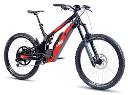
If you’re a serious eBiker who needs a rugged, long-legged, high-performance dual-purpose machine, the LMX 64 might be your new ride of choice. Handcrafted in France by LMX, it features a patented dual-transmission system and an aggressive off-road design that offers an unparalleled riding experience, blending power, range, and lightness for on- and off-road enthusiasts.
When sold in North America, the LMX64 is factory-configured for Class 2 eBike operation, with restricted power (500 W) and a top speed of 20 mph (32 km/h). However, the bike's programmable controller lets off-road riders and racers to unleash much more power (up to 2,500 W) and speed for off-road or competition use.
Innovative eBike Technology and Design
The LMX 64’s patented dual-freewheel transmission sets it apart, enabling the concept of a reliable, powerful, and lightweight off-road speed bike. This system incorporates two independent chains—one for pedaling and one for the motor side—limiting wear and breakage and providing total independence of assistance modes up to 45 km/h. The motorcycle-style, handlebar-mounted throttle adds an element of freedom and control, ideal for navigating obstacles or steep inclines.
Its frame is built with aircraft-grade 6061-T6 aluminum, with components sourced from premium manufacturers that include Rockshox, Bos, Schwalbe, and Formula Cura.
Key features:
- Patented dual transmission: Separate drives for pedal and motor, ensuring precise power delivery and reduced wear.
- Adjustable motor power and speed: Class 2 eBike certification 750 W/20 mph (50 0W in Canada), modifiable to 2,500 W/28 mph for off-road or competition use.
- Advanced battery range: The removable 52-V, 850-Wh battery offers up to 100 km of range in pedal-assist mode and up to 35 km using just the throttle. Maximum charge time is five hours.
- Handlebar-mounted throttle: Provides added control and flexibility, akin to a motorcycle.
- Torque: 171 Nm at the wheel for powerful off-road performance.
- Three riding modes: Riders can choose between three levels of pedal assistance or opt for the motorcycle-style handlebar throttle to propel themselves through city streets and off-road trails.
- Lightweight design: Weighs 29 kg, allowing for easy loading on a bike rack.
- Durable frame: Made from aircraft-grade 6061-T6 aluminum, known for its high resistance to corrosion, stress, and fatigue.
- Accessibility: No need for a motorcycle license.
Perhaps the only downside of the LMX 64 is its price, advertised at $7,499. But, then again, who can put a price on perfection?
Read more articles in the This Week in PowerBites Library Series.


