Digital Isolation Evolves to Meet the Needs of High-Voltage Applications
What you’ll learn:
- The proliferation of high-voltage systems, propelled by the growing demands for electric vehicles, photovoltaic (PV) systems, and industrial control devices.
- The need for more advanced isolators to meet safety standards in high-voltage applications.
- How designers can tackle rising voltage challenges by leveraging innovative digital isolation solutions.
High-voltage systems are becoming increasingly prevalent due to the rising demand for electric-powered vehicles (EVs), photovoltaic (PV) systems, energy storage systems, and industrial control devices. It’s therefore no surprise that advanced isolation ICs are needed more than ever for a wide selection of applications to prevent unwanted currents and system malfunctions.
There are two main types of isolators: optical and digital. Optocouplers use optical characteristics for signal transmission, while digital isolators use either capacitance effects to eliminate interference, or a magnetic field to couple signals across the isolation barrier. Each type has its advantages and drawbacks, depending on the specification requirements. For example, digital capacitive isolators can be the most cost-effective and suitable isolation solution for multichannel designs.
The Need for Advanced Isolation ICs in High-Voltage Systems
As voltages rise, designers are confronted with heightened isolation challenges. The surge in photovoltaic systems' bus voltage to 1,500 V, for instance, necessitates isolators with longer creepage distances to meet safety standards. In addition, the adoption of wide-bandgap (WBG) devices such as silicon carbide (SiC) in various applications adds complexity and increases the requirements for advanced isolators.
Designers working on high-voltage systems will need to address a multitude of additional factors such as isolation rating, creepage distance, common-mode transient immunity (CMTI), and electromagnetic interference (EMI) to ensure power safety, system performance, and reliability in high-voltage systems.
The safety parameters of creepage and clearance are particularly pertinent as designs continue to shrink. There are minimum spacing requirements between metallic contacts external to an isolation device.
Creepage is the shortest distance along solid insulation between two conductive paths, often around the end of the package body, while clearance is the shortest distance through air between two conductive parts, typically measured under the package body. These parameters must be considered to prevent failure or arcing if an electric field passes across the isolator.
Overcoming Isolation Challenges with Innovative Solutions
Designers can address the challenges of rising voltages by leveraging reliable and innovative digital isolation solutions. High-voltage systems often require isolators with a longer creepage distance to meet various international, regional, and national standards, which differ according to the application in question. For instance, in PV power systems, IEC 62109 requires a minimum creepage distance of 14 mm. As a response, some wide-body and even ultra-wide-body packages have emerged.
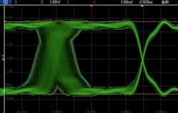
The NOVOSENSE NSI82xx series of high-reliability, multichannel, ultra-wide-body digital isolators was designed to meet the evolving demands of high-voltage systems, featuring extended creepage distances and high electromagnetic immunity (Fig.1). Offering up to 15 mm and high-end EMC properties, they’re well-suited for photovoltaic facilities and other high-voltage systems with high creepage distance requirements.
The digital isolator from this series features UL1577 and CQC safety regulatory certifications, insulation voltage withstand capability of up to 8 kV RMS, and high-speed performance with a data rate of up to 150 Mb/s.
The NSI824x provides digital channel direction configuration and the default output level configuration when the input power is lost. Thanks to a wide supply voltage range, it can be directly connected with most digital interfaces, and allows for easy level shift. Moreover, its system-level EMC performance enhances reliability and stability while in use.
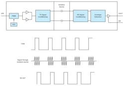
The series adopts the capacitive isolator technology: The digital signal is modulated by the RF carrier generated by the internal oscillator on the transmitter side, then transmitted via capacitive isolator and demodulated on the receiver side. NOVOSENSE’s proprietary Adaptive OOK modulation technology is also used, which offers high noise resistance and low EMI (Fig. 2).
PCB Layout Best Practices for Digital Isolators
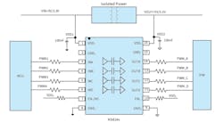
In PCB layout for this type of device, designers must include a 0.1-μF bypass capacitor between VDD1 and GND1, and VDD2 and GND2, placing it as close to the package as possible (Fig. 3).
It’s important to ensure that no planes, traces, bonding pads, or via holes are under the chip in the recommended layout (Fig. 4). For heightened system noise, users can add a series resistor (50 to 300 Ω) on input and output for enhanced robustness, improving latch-up immunity and overall reliability. The isolator drive channel has a typical output impedance of about 50 Ω (±40%), requiring proper termination with a controlled impedance PCB trace if the drive transmission line affects the load.
Overall, digital isolators play an increasingly important role in providing electrical isolation for signal transmission, ensuring the separation of sensitive electronic components from high-voltage elements. These days, they need to offer high operating voltage, low radiation, low power consumption, and high efficiency.
And with applications such as renewable energy and automotive systems going increasingly high-voltage, digital isolators must evolve to meet the corresponding safety requirements. Ultra-wide-body digital isolators will help to ensure power safety, improve system performance, and enhance the overall reliability of these systems.


