The Other Power Transistor Aiming to Dominate the Age of SiC
What you’ll learn:
- Unpacking the challenges with high-voltage power conversion and how SiC fits in.
- The pivotal advantages of SiC over traditional silicon in next-gen power converters.
- Rethinking circuit design for higher efficiency and density in SiC power electronics.
In everything from AI data centers to EV battery chargers, power electronics are under more pressure to perform.
These systems need to handle high voltages and run very efficiently to minimize losses and prevent excess heat generation. At the same time, system-level demands continue to drive higher power density with high-frequency operation. Silicon carbide (SiC) and other new materials for power devices can help solve some of these problems, while more advanced circuit designs can tackle others. But the biggest difference will ultimately come from adopting both.
In data centers, for example, power demands driven by high-performance AI accelerators have reached the point where standard 1U power-supply units (PSUs) need to supply up to 8 kW to server racks. Consequently, they need to take energy from an AC or DC feed operating at several hundred volts and convert it down to 48 V at high current levels for distribution to the individual processor complexes. They need to do so safely, even under fault conditions, and run at high efficiency as power losses cause heat that must be removed.
Meanwhile, the need for high power-supply density calls for reductions in the size and number of capacitors and other passive components that temporarily store energy and smooth out the output of switched-mode power converters. This, in turn, drives the need for higher switching frequencies that can only be fulfilled by a combination of next-gen power transistors and more advanced circuit designs to bring out the best of them.
Reconstruction: The Cascode Unlocks the Power of SiC MOSFETs
Silicon (Si) has dominated the world of power electronics for decades. In combination with circuit designs that optimize high-frequency switching, silicon MOSFETs and IGBTs have evolved to deliver higher power density and efficiency. But existing approaches can only go so far.
SiC is taking over in EV powertrains and other power systems where traditional silicon is struggling. As one of several wide-bandgap semiconductors, SiC is changing the tradeoffs of soft switching and giving power designers more incentive to optimize their approach to power-converter circuit design. A key advantage of SiC lies in its ability to handle high breakdown voltages with very low on-resistance (RDS(on)) per unit area (RDSA).
These benefits are a result of its wider bandgap and higher carrier mobility compared to traditional silicon. This combination makes it easier to design power electronics that can handle distribution voltages reaching 800 V, which is high enough to prevent excessive resistance losses through power-carrying cables, and above. Higher bus voltages also demand transistor designs that can resist strong voltage surges (Fig. 1).
Thanks to the wider bandgap of the underlying semiconductor material, SiC power FETs can use a thinner drift layer that presents less resistance compared to the thicker layers required in traditional silicon devices. The net result is considerably higher conductivity in the on-state.
Using a different transistor design allows you to leverage more of the power of SiC and approach the theoretical limit of on-state resistance versus breakdown voltage. The junction field-effect transistor (JFET), for instance, is designed to deliver a lower intrinsic on-resistance.
>>Download the PDF of this article, and check out the Silicon Carbide (SiC) and Distinguishing Discretes TechXchanges for similar articles and videos
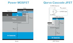
In a standard MOSFET, the carriers must pass across the surface of the p-base, or p-well, region through a resistive inversion channel at the MOS interface before entering the n-type drift region. However, in a JFET, there’s no such inversion channel.
SiC-based JFETs have a power transistor with a greater safety margin with respect to breakdown voltage compared to MOSFET designs, while reducing the on-state resistance per unit area by as much as 50%.
The tradeoff is that, as a normally-on device, the JFET requires a negative voltage to be completely turned off. This is not uncommon in SiC circuitry and may be required for MOSFETs as well to prevent the accidental turn-on of the transistors at temperature extremes where the threshold voltage may fall below nominal levels. However, there’s a way to integrate SiC devices into circuitry that delivers both performance and ease of design.
A cascode configuration enables the SiC JFET to operate in series with a low-voltage silicon MOSFET. In the cascode, a gate driver controls the drain-to-source voltage of the Si MOSFET, which indirectly drives the high-voltage SiC JFET. This configuration gives you a gate-control voltage range that’s compatible with silicon IGBTs, superjunction MOSFETs, and SiC power FETs. As a result, SiC power FETs can be driven with the same gate drivers that are traditionally used to control silicon MOSFETs and IGBTs.
The silicon MOSFET, which exhibits a reduced operating voltage, or the drain-to-source voltage (VDS), contributes less than 10% to the overall on-state resistance of the SiC-based cascode. Coupled with the inherently fast switching speed of SiC, the lower RDS(on) of the JFET enables very high efficiency even at high switching frequency. To simplify power designs, Qorvo is supplying its unique cascode configuration in a single package (Fig. 2).
The Benefits of Zero-Voltage-Switching (ZVS) Architectures with SiC
The cascode’s advantages are most apparent in soft-switching circuit architectures, which are already widely used in power designs based on silicon MOSFETs. The key difference between hard and soft switching is that hard switching has loss contributions from voltage and current overlap during the turn-on and turn-off phases of power transistors. Conceptually, soft switching tunes the timings of the voltage and current swings to reduce the switching losses due to this overlap.
But the reduced parasitics offered by the latest generation of SiC power transistors have allowed designers to turn their attention to the more subtle issues—ones often missed by standard soft-switching techniques.
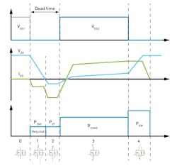
More specifically, many power circuits based on silicon MOSFETs use zero-voltage switching (ZVS). The ZVS approach has the primary purpose of reducing the voltage between the drain and source as the switch turns on and before current begins to flow freely through the channel.
ZVS takes account of the device’s output capacitance, which is the sum of the drain-source capacitance and the capacitance between the gate and drain. This capacitance is normally fully charged after device turn-off in the previous cycle, and it needs to be cleared into the load to avoid losses. Ideally, the current rises to maximum while the voltage across the transistor channel is close to zero (Fig. 3).
ZVS using standard superjunction MOSFETs leads to a period of dead time that can last as long as 300 ns due to the high output capacitance that must be fully charged and discharged during every switching cycle.
At a switching frequency of 500 kHz (2-µs period), a 300 ns dead-time period on both turn-on and turn-off transitions represents 30% of the total duty cycle. Superjunction MOSFETs tend to have strong nonlinearity in their CV curves in this region, as the output capacitance increases significantly at drain-to-source bias of less than 100 V. In a half-bridge topology, this leads to high-voltage transition time near the bus voltage and 0 V during the switching transition.
The 10X lower output capacitance of the SiC JFET compared to that of a silicon MOSFET results in a much shorter dead time. This allows for higher switching frequency, which translates to more power delivery with a higher maximum duty cycle.
Many silicon-based power supplies that implement ZVS suffer from further switching frequency restrictions due to turn-off switching losses. Since it supports much faster switching speeds and, thus, lower turn-off switching losses, SiC can push switching frequency higher in ZVS scenarios. The overall efficiency of the system improves if the fall in current and rise in drain-source voltage during turn-off occur over a short period of time.
Resolving Voltage Spikes, Ringing, and EMI in SiC Power Designs
However, as SiC power devices support higher switching speeds and lower switching losses during turn-off transients, a new challenge—namely, the increased risk of voltage spikes and ringing—comes to the fore.
One method to address this issue is to use high gate resistance (Rg) to slow down device switching speed. But this is unwelcome in designs that aim to use higher frequencies to reduce converter size and cost.
A more effective way to suppress EMI in power supplies—without reducing the switching frequency—is a snubber circuit. The device snubber (Cs) deployed across the device drain-to-source provides peak overshoot control while decoupling capacitors and resistors on the bus (Cd and Rd) provide power loop damping (Fig. 4).
One of the big misconceptions in the electronics industry is that snubber circuits are inefficient. However, for half-bridge topologies typically used in LLC, phase-shifted full-bridge (PSFB), or other power stages that tap into ZVS, a snubber results in higher efficiency compared to having high gate resistance. That’s because the added drain-to-source snubber capacitor doesn’t introduce turn-on loss in ZVS soft-switching applications.
In addition, the current displacement incurred by the drain-to-source snubber capacitor during the turn-off phase will act to decrease the turn-off current of the transistor during turn-off transients. As seen in Figures 5a and 5b, this results in less overlap in voltage and current, which significantly reduces the turn-off loss (Eoff).
A simulation of a 50-kW PSFB topology applying double-pulse testing of a SiC MOSFET module proves my point. Using low-Rg with a drain-to-source snubber Cs to rapidly absorb the voltage spike results in a 50% savings in turn-off switching loss versus the use of high gate resistance.
When replacing the SiC MOSFET module with Qorvo’s JFET-based devices, the snubber delivers another 74% reduction in turn-off switching losses. That, in turn, helps achieve a 10% lower junction temperature at full load.
By holding the junction temperature constant, you can alternatively use the steep reduction in switching losses per cycle to increase the switching frequency—by as much as 3X, according to Qorvo’s testing. That higher frequency further reduces the size of external passive components and the system’s overall cost.
SiC power MOSFETs offers many superior characteristics over silicon. However, to reap the most benefits and achieve the highest performance, engineers should take a closer look at both device selection and circuit topology. The inherent high conductivity of a SiC-based JFET deployed in a cascode configuration such as Qorvo’s can enable dramatic leaps in efficiency by limiting both conduction and switching losses.


