Gravitate to These GaN Apps to Enhance Power Performance
- How to improve power-converter density and efficiency using GaN HEMT in a half-bridge configuration.
- What’s the difference between Direct-Drive GaN and cascoded D-mode GaN designs?
Savvy power design engineers know how to improve power-converter density and efficiency by incorporating gallium-nitride (GaN) devices into their designs. These devices switch faster than silicon MOSFETs, potentially lowering switching losses.
GaN power stages are used in a wide range of applications, such as telecommunications, motor drives, servers, and laptop adapters, and even onboard electric-vehicle chargers.
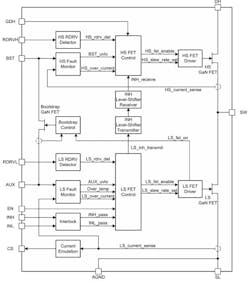
On that front, Texas Instruments offers GaN integrated drivers with protection, such as the LMG2650 GaN half-bridge (Fig. 1), which are targeted at switching power supplies. The 650-V GaN driver FETs in this device can handle the high voltages found in offline power switching applications. The low output capacitive charge reduces both the energy and time necessary for power-converter switching—a critical feature for creating efficient and small power converters.
GaN HEMTs
A GaN device in the depletion mode (D-mode GaN) offers both performance and manufacturing advantages. The normally “on” nature while in this mode during power-up may lead to some abnormal operating conditions. Also, it will require the use of a negative power supply at the gate to turn off.
>>Download the PDF of this article, and check out the TechXchange for similar articles and videos
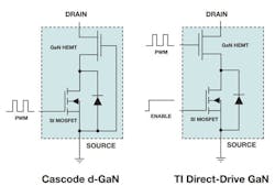
This can be overcome by connecting the D-mode GaN high electron mobility transistor (HEMT) in series with a low-voltage silicon MOSFET in the cascoded D-mode GaN structure. The gate of the HEMT is shorted to the source of the MOSFET, while the HEMT source connects to the drain of the silicon MOSFET (Fig. 2).
Texas Instruments’ solution—TI Direct-Drive—directly drives the GaN HEMT FET, whereby the silicon switch is employed as an enable switch at startup. In this way, the silicon switch doesn’t switch at every cycle, but the GaN switch will do so.
Low-Damage AlGaN/GaN MIS-HEMTs
A low-damage atomic layer etching (ALE) process can enhance the performance of recessed-gate metal-insulator-semiconductor HEMTs (MIS-HEMTs).4 An enhancement-mode (E-mode) AlGaN/GaN recessed-gate MIS-HEMT, with an optimal remaining 5 nm thickness, had state-of-the-art features that included an ID,MAX of 400 mA/mm, a competitive VTH of +2.0 V, an on/off current ratio of 109, and a high breakdown voltage (BV) of 830 V.
The high performance of the recessed-gate MIS-HEMT was achieved not only due to the low-damage ALE process, but also precise etching AlGaN thickness control.
Dielectric Failure Detection and More for GaN Power Transistors
It may surprise readers that GaN power devices face significant challenges with reliability (Fig. 3).5,7
There are three key failure modes caused by HTGB stress:
- Dielectric failure/breakdown resulting from a high electric field in the protection dielectric surrounding the gate. This failure mode is analogous to oxide breakdown mechanisms that occur in MOSFETs.
- Rupture in the gate side wall is an avalanche breakdown mechanism that occurs due to field crowding at the vertical edge of the gate near the gate metal. This failure mode may be controlled via proper surface passivation and electrostatic design.
- Gate bias induced drain leakage current.
GaN, Nuclear Reactors, and Harsh Environments
It’s quite amazing that GaN semiconductors can successfully withstand the harsh environment close to a nuclear reactor core. Why is this important?
This discovery might make it possible to locate GaN electronic components closer to sensors within an operating nuclear reactor. It will ultimately lead to more accurate and precise measurements in more compact designs.
This means that not too far in the future, wireless sensors will be able to operate within nuclear reactors. This includes small advanced modular and microreactor designs that are currently under development.
References
1. Gallium Nitride (GaN) Power Stages, Texas Instruments.
2. “Design considerations of GaN devices for improving power-converter efficiency and density,” Salil Chellappan, Power Density Industrial Systems, Systems Manager, Texas Instruments, November 2017.
3. “Nomenclature, Types, and Structure of GaN Transistors,” Hagar Mohamed, SLUAAM1, Texas Instruments, August 2022.
4. “Investigation of AlGaN/GaN MISHEMTs with Varied AlGaN Barrier Depths via a Low Damage ALE Process,” An-Chen Liu, Hsin-Chu Chen, Po-Tsung Tu, Sung-Jin Cho, Andrew Newton, Yung-Yu Lai, Yan-Lin Chen, Po-Chun Yeh, Shu-Tong Chang, and Hao-Chung Kuo, Fellow, IEEE, 2024 International VLSI Symposium on Technology, Systems and Applications (VLSI TSA), 2024.
5. “Dielectric Reliability in GaN Metal-Insulator-Semiconductor High Electron Mobility Transistors,” Ethan S. Lee. Thesis submitted to the Department of Electrical Engineering and Computer Science on August 28, 2018, in partial fulfillment of the requirements for the degree of Master of Science, 2018.
6. “A 10 MHz GaN Driver IC with Bang-Bang Dead Time Control for Synchronous Rectifier Buck Converter,” Pin Ying Wang, Ping Kun Chiu, Sheng Teng Li, Sheng Teng Li, Chih Chao Hsu, IEEE 2020.
7. “eGaN Technology Reliability and Physics of Failure—How eGaN FETs are expected to behave as the result of high gate voltage stress conditions,” GaN Talk, EPC, February 3, 2017.
>>Download the PDF of this article, and check out the TechXchange for similar articles and videos
About the Author

Steve Taranovich
Freelance Technical Writer, Phoenix Information Communication LLC
Steve is a contributing editor to Electronic Design.
Author of the non-fiction “Guardians of the Right Stuff,” a true story of the Apollo program as told by NASA and Grumman Corp. engineers, an astronaut, and technicians.
Experienced Editor-In-Chief of EETimes/Planet Analog and Senior Technical Editor at EDN running the Analog and Power Management Design Centers from 2012 to 2019.
A demonstrated history in electronic circuit design and applications for 40 years, and nine years of technical writing and editing in industry. Skilled in Analog Electronics, Space-related Electronics, Audio, RF & Communications, Power Management, Electrical Engineering, and Integrated Circuits (IC).
1972 to 1988 worked as a circuit design engineer in audio (8 years) and microwave (8 years). Then was Corporate Account Manager/applications engineer for Burr-Brown from 1988 to 2000 when TI purchased Burr-Brown. Worked for TI from 2000 to 2011.
Strong media and communication professional with a BEEE from NYU Engineering in 1972 and an MSEE from Polytechnic University in 1989. Senior Lifetime member of IEEE. Former IEEE Long Island, NY Director of Educational Activities. Eta Kappa Nu EE honor society member since 1970.


