GaN Power Transistors: Master Strokes on a Power-Supply Canvas (.PDF Download)
It’s not news that the efficiency of switching power supplies is now above 90% in many applications. At those levels, it becomes progressively harder to eke out small improvements.
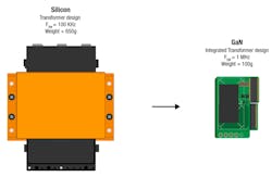
The introduction of power devices made from wide-bandgap (WBG) semiconductors such as gallium nitride (GaN) and silicon carbide (SiC), instead of silicon, has given designers some important new tools (Fig. 1).
1. Changing from silicon to GaN in a power supply can slash the size of magnetic components such as transformers. (Source: TI: “Gallium Nitride (GaN): Pushing performance beyond silicon”)
In a power supply, changing from silicon MOSFETs to transistors based on gallium nitride (GaN) yields efficiency improvements. A GaN device (Fig. 2) has lower on-resistance RDS(ON) than a silicon device. It also has a higher breakdown voltage, can operate at higher temperatures, and has far superior reverse-recovery characteristics. The GaN device also incurs much lower switching losses, so it can operate at higher switching frequencies. As shown in Fig. 1, this can lead to a dramatic reduction in the size of the design.

