Bi-Directional Controller IC Employs Supercapacitors For DC Power Backup
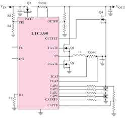
Power outages lasting just a few seconds can impact a system’s operating functions and also cause a loss of important data. In the past, a UPS (uninterruptible power supply) might have been used as a power backup, but it is overkill for short duration outages and requires constant attention to its batteries. Now, there is Linear Technology’s LTC3350, a mixed-signal power controller IC that can charge and monitor a series stack of one to four supercapacitors and then provide a several seconds of power backup (depending on the total capacitance and the load). In a typical system configuration, the LTC3350 mates with another circuit in order to provide it with dc backup power if it experiences a short duration power outage. The LTC3350 is available in a low profile 38-lead 5mm × 7mm × 0.75mm QFN surface mount package. Fig. 1 is a simplified schematic of an LTC3350 application.
Related Articles
- Control IC Regulates Lamp Ballasts
- Controller IC Employs Real-Time Adaptive Loop Compensation, PMBus
- Lithium-Ion Battery Charge Controller IC Regulates Mobile Devices
- Buck-Boost Battery Charging Controller Handles 55 V
- Flyback Controller IC Integrates Power Factor Correction
- Control IC Regulates Lamp Ballasts
Functions performed by LTC3350’s bi-directional switching controller include:
1. Charging one to four supercapacitors
2. In case of an associated circuit’s power failure, delivering dc voltage stored in the supercapacitors to the circuit input
3. Monitors system voltages, currents, and die temperature.
4. Balancing and providing overvoltage protection for the supercapacitors
5. Providing seamless power path control
6. Employing its I2C interface for data monitoring and capacitor charge control
The PFI pin is a Power-Fail Comparator input whose threshold voltage is programmed by an external resistor divider (R1 and R2) via the PFI pin. If VIN is above the externally programmable PFI threshold voltage, the synchronous controller operates in step-down mode and charges a stack of supercapacitors that store the maximum charge voltage. If VIN goes below the PFI threshold (for example, zero volts) then the synchronous controller runs in reverse as a step-up converter to deliver the stored supercapacitor stack voltage that provides the backup power.
In the charge mode, charging proceeds at a constant current until the supercapacitors reach their maximum charge voltage determined by the CAPFB servo voltage and the resistor divider between VCAP and CAPFB. The maximum charge current is determined by the value of sense resistor, RSNSC, in series with the inductor. The charge current loop servos the voltage across the sense resistor to 32mV. When charging begins, an internal soft-start ramp increases the charge current from zero to full current in 2 ms.
The LTC3350 provides constant power charging (for a fixed VIN) by limiting the input current drawn by the switching controller in step-down mode. The input current limit reduces charge current to limit the voltage across the input sense resistor, RSNSI, to 32 mV. If the combined system load plus supercapacitor charge current is large enough to cause the switching controller to reach the programmed input current limit, the input current limit loop will reduce the charge current by precisely the amount necessary to enable the external load to be satisfied.
IF input power is lost, the bidirectional switching controller acts as a step-up converter to provide power from the supercapacitors to VOUT, which becomes the backup power for the mating circuit. A resistor divider between VOUT and OUTFB sets VOUT regulation. The step-up mode can be used in conjunction with the output ideal diode. The VOUT regulation voltage can be set below the capacitor stack voltage. Upon removal of input power, power to VOUT will be provided from the supercapacitor stack via the output ideal diode. VCAP and VOUT will fall as the load current discharges the supercapacitor stack.
Two ideal diode controllers drive external N-channel MOSFETs (Q3 and Q4). The ideal diodes consist of a precision amplifier that drives the gates of N-channel MOSFETs whenever the voltage at VOUT is approximately 15 mV below the voltage at VIN or VCAP. Within the amplifier’s linear range, the small-signal resistance of the ideal diode will be quite low, keeping the forward drop near 15 mV. At higher current levels, the MOSFETs will be in full conduction.
The input ideal diode prevents the supercapacitors from back driving VIN during backup mode. A Fast-Off comparator shuts off the N-channel MOSFET if VIN falls 30 mV below VOUT. The PFI comparator also shuts off the MOSFET is there is a power failure.
The output ideal diode provides a path for the supercapacitors to power VOUT when VIN is unavailable. In addition to a Fast-Off comparator, the output ideal diode also has a Fast-On comparator that turns on the external MOSFET when VOUT drops 45 mV below VCAP.
Balancing Supercapacitors
The LTC3350 provides balancing and overvoltage protection to the series stack of supercapacitors. The internal capacitor voltage balancers eliminate the need for external balance resistors. Overvoltage protection is provided by shunt regulators that use an internal switch and an external resistor across each supercapacitor.
There is an integrated, active stack balancer that slowly balances all the capacitor voltages to within about 10 mV of each other. This maximizes the life of the supercapacitors by keeping the voltage on each as low as possible to achieve the needed total stack voltage.
If the difference between any two capacitor voltages exceeds about 10 mV, the capacitor with the largest voltage is discharged with a resistive balancer at about 10 mA until all capacitor voltages are within 10mV.
Besides balancing, each capacitor must be protected from overvoltage during charging. The capacitors in the stack will not have exactly the same capacitance due to manufacturing tolerances or uneven aging. Therefore capacitor voltages can increase at different rates with the same charge current. If this mismatch is severe enough or if the capacitors are being charged to near their maximum voltage, it becomes necessary to limit the voltage increase on some capacitors while still charging the other capacitors. Up to 500 mA may be shunted around a capacitor whose voltage is approaching the programmable shunt voltage. This shunt current reduces the charge rate of that capacitor relative to the other capacitors.
If a capacitor continues to approach its shunt voltage, the charge current is reduced. This protects the capacitor from overvoltage while still charging the other capacitors, although at a reduced rate of charge. The shunt voltage is programmable in 183 μV increments up to 3.6 V.
An integrated 14-bit sigma-delta analog-to-digital converter (ADC) is automatically multiplexed between 11 measurement channels. Its results are stored in registers accessible via the I2C/SMBus port. Each ADC channel takes approximately 820 μs for a measurement. Besides providing status information about the system voltages and currents, some of these measurements are used by the LTC3350 to balance, protect, and measure the capacitors in the stack.
The LTC3350 can also measure the capacitance and equivalent series resistance (ESR) of its supercapacitor stack. This measurement is performed with minimal impact to the system, and can be done while the supercapacitor backup system is online. This measurement discharges the capacitor stack by a small amount (200 mV).
The capacitance test is performed only once the supercapacitors have finished charging. The test temporarily disables the charger, then discharges the supercapacitors by 200 mV with a precision current. The discharge time is measured and used to calculate the capacitance with the result of this measurement stored in a register. The number reported is proportional to the capacitance of the entire stack.
The ESR test is performed immediately following the capacitance test. The switching controller is switched on and off several times. The changes in charge current and stack voltage are measured. These measurements are used to calculate the ESR relative to the charge current sense resistor. The result of this measurement is stored in a register.
The LTC3350 monitors system voltages, currents, and die temperature. The ADC monitors the integrated die temperature sensor and sends the digitized value to a register. An alarm may be programmed for the die temperature high temperature limits.
A general purpose input (GPI) pin is also available to measure additional system parameters. In addition, the LTC3350 can measure the capacitance and resistance of the supercapacitor stack. This provides indication of the health of the supercapacitors and, along with the VCAP voltage measurement, provides information on the total energy stored and the maximum power that can be delivered. The voltage on this pin is directly digitized by the ADC. For high impedance inputs, an internal buffer may be selected and used to drive the ADC.
To monitor the temperature of the supercapacitor stack, the GPI pin can be connected to a negative temperature coefficient (NTC) thermistor. A low drift bias resistor is required from INTVCC (internal 5 V regulator) to the GPI pin and a thermistor is required from GPI to ground. Connect GPI to GND if not used.
Resistor, RT, from the RT pin to ground sets the switching frequency. RT also sets the scale factor for the capacitor measurement value.
Communication
An I2C/SMBus port allows a host computer to communicate with the LTC3350 for configuration and reading back telemetry data. The port supports two SMBus formats, read word and write word. The registers accessible via this port are organized on an 8-bit address bus and each register is 16 bits wide. The “command code” (or sub-address) of the SMBus read/write word formats is the 8-bit address of each of these registers.
Although the LTC3350 has extensive digital features, only a few are required for basic use. The shunt voltage should be programmed via a vshunt register if a value other than the default 2.7 V is required. Other digital features are optional and used for monitoring.
The ADC automatically runs and stores conversions to registers. Capacitance and ESR measurements only run if requested, however, they may be scheduled to repeat if desired. Each measured parameter has programmable limits, which may trigger an alarm. Most alarms are normally disabled.
This system may use from one to four supercapacitors. If less than four capacitors are used, the capacitors must be populated from CAPRTN to CAP4, and the unused CAP pins must be tied to the highest used CAP pin. For example, if three capacitors are used, CAP4 should be tied to CAP3. If only two capacitors are used, both CAP4 and CAP3 should be tied to CAP2. The number of capacitors used must be programmed.
MOSFETs
Use logic-level threshold N-channel MOSFETs for Q3 and Q4. Select MOSFETs with a low enough RDS(ON) to obtain the desired VDS while operating at full load current. The LTC3350 will regulate the forward voltage drop across the input and output ideal diode MOSFETs to 30 mV if RDS(ON) is low enough. The required RDS(ON) can be calculated by dividing 0.030V by the load current in amps.
Achieving forward regulation minimizes power loss and heat dissipation, but it is not a necessity. If a forward voltage drop of more than 30 mV is acceptable, then a smaller MOSFET can be used but must be sized compatible with the higher power dissipation. Take care to ensure that the power dissipated is never allowed to rise above the manufacturer’s recommended maximum level.
The body diode of the output ideal diode N-channel MOSFET will carry the load current until VCAP drops to within a diode forward drop of the VOUT regulation voltage at which point the synchronous controller takes over. During this period the power dissipation in the output ideal diode MOSFET increases significantly. Diode conduction time is small compared to the overall backup time but can be significant when discharging very large supercapacitors (>600 F). Care should be taken to properly heat sink the MOSFET to limit the temperature rise.


