Minimizing Power-Supply Voltage Drop on PCBs
Despite the widespread availability and use of low-power components, today’s printed circuit boards (PCBs) can require a significant amount of current, with boards drawing 50, 100, and even 200 A in common use. Whenever current is delivered to a load, there will be IR-based voltage drop, and designers must take this loss into account when laying out the board and placing the supply, dc supply rails, and loads.
For consistent and reliable operation, it’s important to ensure this drop doesn’t push these dc rail voltages to the lower end of their minimum/maximum band. Typically, it’s plus/minus a few percent of the nominal value.
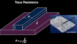
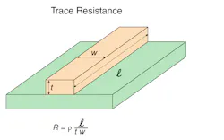
A quick look at the numbers clarifies the challenge. Standard “1-oz.” copper (so called because it weighs 1 oz. per square foot) on a PCB laminate such as FR-4 has a thickness of 35 µm; 2-oz. copper is twice as thick, of course, and “thin” copper is half as thick. Using 1-oz. copper as an example, a 10-cm long, 1-mm-wide trace will have a resistance of about 50 mΩ (the resistivity of copper is 1.74 × 10⁻⁸ Ω⋅m at 20°C). There are many handy online resistance calculators for this, such as the one at Trance-Cat (Fig. 1).
If you are delivering 10 A through this trace, the IR drop is about 500 mV (0.5 V), which is substantial. This means the dc rail at the load is one-half volt lower than it is at the supply, and there’s also wasted power (I2R) and accompanying heat dissipation. Note that the drop isn’t a function of the nominal voltage value of the rail—it depends only on the current and resistance. Therefore, a 15-V rail sees the same loss as a 3-V rail, but the proportional loss is far greater at the lower voltage.
The situation can get even worse. Some designs use a low-resistance ground plane (often as a distinct PCB layer) for both analog and digital signal grounds and dc power-return ground. However, many designs benefit from (or require) separate ground paths for the signals and for power ground to minimize noise, and may even use a separate dc-return path. In such cases, the IR drop is effectively doubled, with one drop for the supply output rail to load, and a second drop for the load return of the current to the supply.
Overcoming IR Drop
Designers have several choices to minimize IR drop:
- Use a higher-voltage dc rail, such a 48 V or 12/12 V dc in an intermediate bus converter (IBC) arrangement, then use multiple local, point-of-load (PoL) dc-dc converters placed close to their respective loads. This solves the IR drop problem (and greatly reduces noise pickup in the rails as well), but costs in more dc-dc converters and PCB real estate. Despite this, it’s a widely used and effective solution.
- Adjust the nominal dc supply value up to pre-compensate for the IR drop. This is a somewhat-effective “workaround,” but also brings some risks.
--Some otherwise very good or preferred supplies aren’t adjustable, so they must be ruled out of consideration.
--If the load current demand drops during use (as it almost always does), the IR drop will decrease as well, and the supply could actually deliver a rail voltage which is too high.
--If a supply must be replaced in the field, the replacement may not be set at the compensated voltage or be misadjusted, leading to a non-functioning circuit or one that’s intermittent.
- Use remote sensing, a variation on Kelvin sensing that some supplies support. The supply has two additional leads, so it can sense the voltage at the load and dynamically adjust its output to maintain that value despite IR drop and load shifts. This is effective but also has drawbacks:
--The dynamic response of the sensing feedback loop may not be fast enough to compensate, or it may be too fast, overshoot, and oscillate.
--The sensing leads form a physically large feedback loop that may pick up system noise and thus cause the supply to misread the sensed value; again, this can even induce oscillation of the supply rail.
Consider Other Solutions
All of these options are in use, and all of them can work under well-defined and controlled conditions, but they’re all “workarounds” and “patches” for the technically better and more robust solution of minimizing their drop in the first place. Again, there are options and tradeoffs:
- Use thicker copper cladding; 2 oz. and even 3 oz. are available. Doubling the thickness halves the resistance, but doing so adds to the cost of the raw PCB material and adds board weight; puts more copper where it isn’t needed; and increases as fabrication time due to extra time needed for chemical etch or additive plating—the two ways a PCB’s copper paths can be created.
- Use wider PCB traces; again, doubling the width halves the resistance. However, the cost is additional PCB “real estate” for these DC rails and their ground returns. Some advanced layouts use wider traces as much as possible, but also narrow them to get around obstacles and tight-clearance areas on the board, as a sort of compromise. If a 10-cm run is narrow only over one centimeter of the run, the increase in resistance obviously only occurs on that short segment.
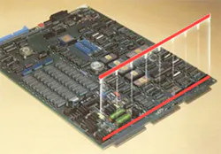
- Use a stand-up busbar (also spelled as buss bar or bus bar), to route the power, thus using the unused z-axis (height) dimension. Even if the board is a low-profile SMT design, there’s usually headroom for a low-profile bus bar that can be relatively thick, and so it provides a low-resistance dc path. Many of these bars are offered as two-layer (or more layers) structures, with one layer for the supply rail or rails and the other for the ground return. The cost is just the BOM component cost—the impact on the PCB itself is minimal as these don’t require thicker copper, wider traces, or other workarounds.
Busbars come in a wide range of thicknesses, heights layers, pin spacings, and lengths. For example, one busbar offered by E-Fab has two copper layers separated by an insulator (Fig. 2). The layers have a staggered PCB pin configuration so that the pins alternate power and ground.
Busbars provide another “free” benefit: They stiffen the PCB against flexing, which is a consideration with larger boards or for those in vibration environments (mil/aero, automotive, and many others). Some designs use a busbar only for the higher-current loads such as MOSFETs or IBGTs. This reduces their modest cost and eases layout issues (if any) associated with bu bars while maximizing their effectiveness.
Conclusion
From an electrical-only perspective, ensuring that the full nominal voltage from the supply reaches the load, and does so with insignificant IR voltage loss or I2R power dissipation, is critical for reliable, non-intermittent performance. Each solution to the issue has tradeoffs, and there’s no single best answer, but the downsides of each should be carefully understood and assessed.


