"Bolt-On" Circuit, Transistors Create Zero-Drift Current Source
This file type includes high-resolution graphics and schematics when applicable.
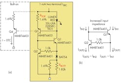
A two-terminal current source using the basic circuit of Figure 1a can be enhanced by adding on an independent subcircuit that uses degeneration of a PNP transistor to achieve zero temperature coefficient (tempco or TC). This low-cost design is the result of collecting data on many semiconductor devices over a 15+ year period and frequent reviews of the data. ("Degeneration" is the insertion a resistor in series with the emitter, which decreases the gain of the amplifier but improves attributes such as linearity and input impedance.)
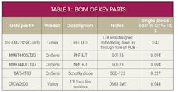
The key semiconductors in the bill of materials (BOM) of Table 1 are critical to this circuit, so design and test only with these parts. The choice of parts and their vendor makes this design viable, and the circuit has been built over various lots of material with parts purchased from different distributors. Both the MMBT4401 and the MMBT4403 transistors should each come from their own, single tape reel of parts.
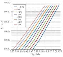
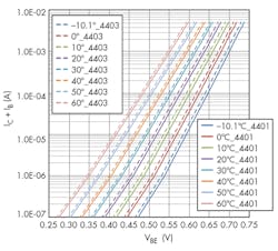
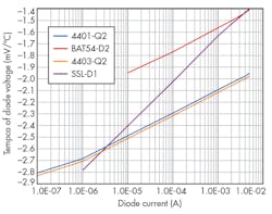
Audio-design engineers have known for years that ON Semiconductor’s MMBT4401 and MMBT4403 feature very low base resistance (Rb) and thermal noise, and are very good for current-source and mirror circuits. The MMBT4401 and MMBT4403 are complementary devices related to dc biasing and tempco. (Figs. 10 and 11 in Appendix below). Complementary devices make it easier to understand the zero tempco design as a “glue” circuit needs to pass the current from the PNP device Q3 of its mirror to Q2. The base-to-emitter voltages VBE will be approximately equal in those two transistors.
The design is fault-tolerant and can be reverse-biased. For industrial designs at higher supply voltages, the majority of the forward voltage drop is across the collector/base of Q1 and Q3, the top MMBT4401 and MMBT4403 devices, with a 40-V BVCBO (the collector-to-base breakdown voltage with open-circuit emitter). A series resistor can be used for surge protection, with a penalty in voltage headroom.
A compact printed-circuit-board (PCB) layout is needed to prevent thermal gradients. The LED "photoelectric effect" has been found to not be an issue here, as the LED is the type where the LED lens is pointing down when mounted in the PCB. Light-tolerance testing has also been performed. Viewing the LED from the die-mount side of its package shows a red glow and can be used as a visual indicator that the current source is functional.
Figure 1b is the “glue” circuit using two each of MMBT4401 NPN devices and 1.0-kΩ resistor. It connects a top current mirror and a bottom current mirror. The two key design equations for the add-on circuit are:
IE(Q2) ~ IIN2, therefore:
IE(Q2)/IIN2 = IE(Q2)/[IC(Q2) + IB(Q1)] = (1 + 1/β)/[1 + IB(Q1)/IC(Q2)] = (1 + 1/ β)/(1 + 1/ β) = 1
IOUT1 ~ IC(Q1), therefore:
IOUT1/ IC(Q1) = [IC(Q1) × (1 + 1/β) – IC(Q2)/β]/ IC(Q1) = 1 + 1/β – [1/β × [IC(Q2)/IC(Q1)]] = 1
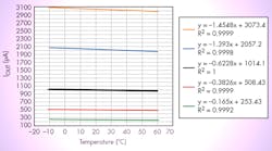
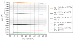
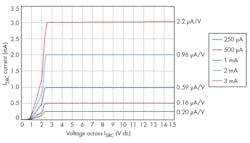
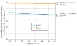
Figure 2 shows the current-source values and their change with temperature, while the steady-state performance over input voltage and the minimum operating conditions are shown in Figure 3. The tempco of the bolt-on circuit (Fig. 4) compares favorably with the REF200, a commercially available, precision, dual-current source/current sink. That device has a temperature coefficient of ±25 ppm/°C on its fixed 100-μA current source.
However, this current source can be set to any desired current and costs significantly less than the REF200. Also, the typical capacitance of the REF200 is 10 pF, while the value for this current source is less than 10 pF, and the typical output impedance of a REF200 is 100 MΩ from 2.5 V to 40 V. The two-terminal current source is a very repeatable, low-cost circuit and is a viable choice for replacing certain commercial ICs providing the same function.
APPENDIX
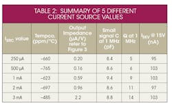
Table 2 summarizes key information from Figures 2 and 3 and from additional measurements. The ISRC tempco is intentionally designed to be significantly less than PTAT, which is –3300 ppm/°C. For the two-terminal ISRC, the strongest effect to absolute value of current is temperature. The effect of applied voltage causes less change.
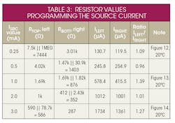
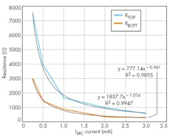
Figure 5 empirically helps determine resistor values for other current source values.
I/V Plot Used for Design of Different Current-Source Values
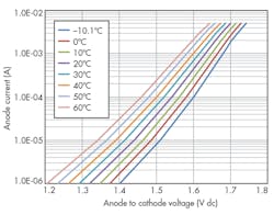
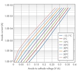
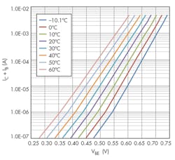
I/V plots of Figures 6, 7, 8 and 9 are used to design new two-terminal current-source values. The semiconductor devices for these plots were randomly selected and never placed into a current source. The bottom two-terminal current mirror of the MMBT4401, BAT54, and RBOTT is designed first. Then the top two-terminal current mirror of the MMBT4403, RED LED, and RTOP is designed next. This top mirror circuit is very familiar to designers, as it has been around for many decades.
The BAT54, MMBT4401, and MMBT4403 results are very linear on their log scale.
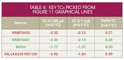
The most notable point from Figure 11 is that the TC of the BJTs is essentially the same at a given current. The BAT54 has a lesser TC than the BJTs.
Note the delta TCs in Table 4. All are identical except the RED LED, which is double the others.
Calculations for Two-Terminal ISRC (and introducing the 0TC left leg)
A total current source value is picked. The left-side current is made to be greater than the right-side current value by a ratio of approximately 1.3 to 1.4.
MMBT4401 (Q2) in parallel with BAT54T/RBOTT:
As the temperature increases, the MMBT4401 (Q2) voltage decreases quicker than that of the BAT54. Therefore, the current decreases through RBOTT and results in a negative TC. If the TC of the BAT54T equaled that of the MMBT4401 (Q2), the TC of the current through R1 would be 0. This tempco accounts for the majority of the tempco for the ISRC. The BAT54T and RBOTT are in series; for biasing purposes, the lower Schottky voltage drop gives a significant voltage value across the resistor to set a current.
RED LED in parallel with MMBT4403 (Q3)/RTOP:
As temperature goes up, the MMBT4403 (Q3) voltage decreases only slightly quicker than the LED’s voltage, and the LED makes up for this voltage amount by having a current with a negative tempco biasing it. The TC of the current in the left leg is approximately 0 µA/°C.
Regarding TCs, the MMBT4403 (Q3) and the lower left MMBT4401 (Q2) will have similar TCs. The TC of the MMBT4403 (Q3) and the effective TC of the LED will have similar TCs. The example of Table 5 and the following calculations demonstrate the use of the figures and the math. The values in Table 5 are similar to the data in Figure 4. This result also supports the 0TC for the current in the left leg of the two-terminal ISRC.
TC of right current = (390-417)/1000/(60-20)*106 = –675 ppm/°C
TC of MMBT4403 (Q3) = (0.53-0.62)/(60-20) = –2.25 mV/°C
TC of MMBT4401 (Q2) = (0.53-0.62)/(60-20) = –2.25 mV/°C
Effective TC of VLED = (1.515-1.605)/(60-20) = –2.25 mV/°C (change in current included)
Effective TC of Schottky = (0.188-0.255)/(60-20) = –1.68 mV/°C (change in current included)
Measured Data with 0TC in Left Leg and Bolt-on pnp to Harvest 0TC Current
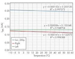
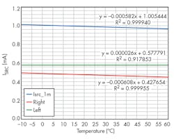
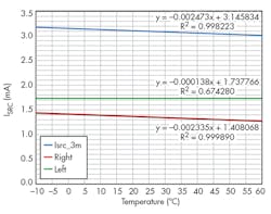
The 0TC current in the left leg of the circuit has been shown to work in the current range of two-terminal ISRC values from 250 µA to 3 mA. This is demonstrated in three plots (Figs. 12, 13, and 14). At this time, there’s no trimming method for the TC. The fit for the “left” side current is best fit by a quadratic. A linear fit is used in these plots. Figures 12, 13 and 14 are plots from the 250-µA, 1-mA, and 3-mA ISRCs, respectively.
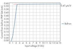
Figure 15 is measured from the same ISRC circuit as Figure 4. The figure shows the output impedance of the degenerated pnp, and the effective early voltage is given.
Tim Davis graduated with a BSEE from Iowa State University in Ames, Iowa. He has more than 28 years of experience in analog circuit design, power electronics, and IC design, including several patents for electronics in the medical industry. He can be reached at [email protected].
Looking for parts? Go to SourceESB.
