Minimize the EMI in Your Power Supplies
Members can download this article in PDF format.
What you’ll learn:
- Some handy methods to reduce EMI levels in power supplies.
- EMI sources in a switch-mode power supply.
- The importance of PCB layout in diminishing EMI.
Modern electronic systems are becoming progressively denser with a high level of integration. This article will present some tried and true methods to reduce electromagnetic interference (EMI) levels in power-supply system designs. Designers must be aware of serious EMI setbacks when they’re in the late stages of the design phase, which could otherwise lead to excessive costs in money and time.
This article discusses how to improve EMI in terms of filter size and cost while reducing design time and complexity, especially in switch-mode power supplies (SMPS).
The switching effect in power metal-oxide semiconductor field-effect transistors (MOSFETs) leads to a significant source of EMI in the system. This effect will ultimately impact system reliability.
EMI mostly appears from discontinuous input currents, high slew rates on switching nodes, and more ringing on switching edges that’s caused by parasitic inductances within the power loop.
Sources of EMI in an SMPS
EMI can’t be addressed late in the circuit design phase, because it could lead to setbacks in cost and time.
For example, consider the buck converter in Figure 1. It demonstrates how each element reveals itself within various frequency bands.
To reduce the cost and size of the SMPS, designers are presently trying to increase switching frequencies, which will also enhance efficiency. However, this shift to higher switching frequencies will lead to more EMI problems. Now designers will need to freely integrate EMI mitigation methods that will not compromise the power-supply design.
The above rules are well established in industry-standard specifications like Comité International Spécial des Perturbations Radioélectriques (CISPR) 25 for the automotive industry, and CISPR 32 for multimedia equipment. Interference will be limited to a particular level, and susceptible circuits will be capable of handling that level of interference.
Approaches for Reducing Interference
Designers must know the applicable standard for each given application. Also important is to understand how to measure EMI, since this knowledge will give engineers better insight into reducing EMI.
In automotive design that involves long wire harnesses, conducted EMI relates to their increasing number in the latest vehicles. Some of the best ways to prevent or mitigate EMI:
Shielding
This is likely the best means to contain coupling or radiation EMI. Shielded metal housings and coatings can be used. Also, cables should be shielded to prevent external EMI from affecting sensitive components.
Filtering
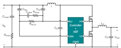
Employ filters to eliminate unwanted signals. Passive filters may be frequently employed to minimize EMI. Also, an AC line filter may prevent undesirable signals from entering the power supply or other powered circuitry. An integrated active EMI filter will help lower differential-mode (DM) conducted emissions at the input to a system, because it can serve as a very effective low impedance shunt (Fig. 2).
Ferrite beads can also suppress high-frequency noise.
Grounding
Grounding typically provides a low impedance path for EMI. When a system is properly grounded, EMI is diverted from critical equipment, improving power quality. Be sure to use proper grounding on a printed circuit board (PCB) and keep trace lengths short and away from PCB edges if possible. Also, minimize loop areas on the PCB to reduce radiated emissions.
Twisted-pair cables can help to reduce common-mode noise, too.
More Layout Tips
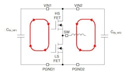
Let’s look at the PCB layout for a typical DC-DC buck converter, which is crucial to optimal performance. The PCB layout is a crucial factor in achieving optimum EMI performance of the converter. In the buck converter, the loop formed by the input capacitor(s) and power ground is the most critical area. This loop will have large transient currents that lead to high transient voltages when they react with trace inductance.
Designers must be aware of the traces in this loop, which must be wide and short. The loop area also must be as small as possible to reduce parasitic inductance (Fig. 3). Complete layout guidelines are given in Reference 2.
Avoiding EMI Disruption
EMI in a design can ruin a designer’s day. It crops up when electromagnetic fields, which are generated by electrical/electronic systems, interfere with one another. This may lead to serious disruptions in circuitry, thus causing interruptions that can affect nearby electronic devices. A variety of methods can be applied to minimize EMI, as discussed in this article.
Read more articles in the TechXchanges: Delving into EMI, EMC, and Noise and Power Supply Design.
References
1. “Time-Saving and Cost-Effective Innovations for EMI Reduction in Power Supplies,” Yogesh Ramadass, Ambreesh Tripathi, Paul Curtis, Texas Instruments, December 2023.
2. “LMQ61460-Q1 Automotive 3-V to 36-V, 6 A, Low EMI Synchronous Step-Down Converter,” Texas Instruments, SNVSBP4C, March 2020 (revised January 2021).
3. “Advanced Power-Converter Features for Reducing EMI,” Orlando Murray, Analog Applications Engineer, Wide Input Buck Switching Regulators; Jimmy Hua Analog Applications Engineer Wide Input Buck Switching Regulators, Texas Instruments.
About the Author

Steve Taranovich
Freelance Technical Writer, Phoenix Information Communication LLC
Steve is a contributing editor to Electronic Design.
Author of the non-fiction “Guardians of the Right Stuff,” a true story of the Apollo program as told by NASA and Grumman Corp. engineers, an astronaut, and technicians.
Experienced Editor-In-Chief of EETimes/Planet Analog and Senior Technical Editor at EDN running the Analog and Power Management Design Centers from 2012 to 2019.
A demonstrated history in electronic circuit design and applications for 40 years, and nine years of technical writing and editing in industry. Skilled in Analog Electronics, Space-related Electronics, Audio, RF & Communications, Power Management, Electrical Engineering, and Integrated Circuits (IC).
1972 to 1988 worked as a circuit design engineer in audio (8 years) and microwave (8 years). Then was Corporate Account Manager/applications engineer for Burr-Brown from 1988 to 2000 when TI purchased Burr-Brown. Worked for TI from 2000 to 2011.
Strong media and communication professional with a BEEE from NYU Engineering in 1972 and an MSEE from Polytechnic University in 1989. Senior Lifetime member of IEEE. Former IEEE Long Island, NY Director of Educational Activities. Eta Kappa Nu EE honor society member since 1970.


