Designing R2CD Snubbers Using Standard Recovery Diodes
Snubbers play an important role in switch-mode power supplies. To understand use of the snubber, we have to look at the performance of a switch-mode power supply.
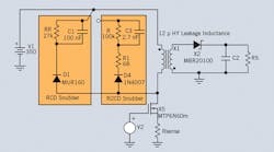
Fig. 1. RCD and R2CD snubbers for ON Semi Demo, NCP1216 70 Watt Flyback
Fig. 1 illustrates the two types of snubbers used in a switch-mode power supply: RCD and R2CD. When a switch-mode power supply, SMPS, switches OFF, the parasitic leakage inductance [1] that couples the primary and secondary winding of a transformer must be charged or discharged. In that brief instant, the resulting voltage transient must be stabilized to prevent circuit destruction caused by the sudden change in current transmitted to the leakage inductance.
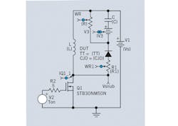
The test circuit shown in Fig. 2 describes the snubber circuit.
Fig. 2. Snubber test circuit examines theory
Common Diode Data
FET, Q1, charges the simulated leakage inductance when it is turned ON and releases the charge into the snubber circuit when it is turned OFF. The parameter blocks in Table 1 represent either RCD or R2CD (used when reverse recovery time, trr, is > .5 microseconds) configurations.
Snubber parameters are adjusted for each case to yield the same results. The FET should be the same device used in the final design in order to account circuit affects imposed by the actual device. The drain voltage reaches about 2 kV using this test circuit when the snubber is removed and avalanche does not occur.
If the snubber diode is conducting reverse current when it turns OFF, a negative transient voltage spike occurs at Q1 drain (typical RCD behavior). This spike results from discharging the residual leakage inductor current into Q1 and results in a damped ringing behavior when switch capacitance is included in the model. However, if a long trr diode is used, it’s possible to design the circuit so that the current is zero when the diode drops out of conduction; a high efficiency resonant condition.
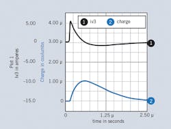
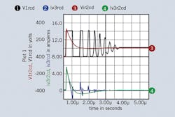
Standard recovery diodes exhibit a long storage time that is characterized as trr in the data sheets. By convention, the standard recovery diodes have trr specified as greater than 0.5 µS; trr typically ranges from 2 µS to 5 µS, increasing with higher voltage rating. When the transient current in the snubber diode is shorter than trr, the stored charge can be removed just as the diode voltage approaches zero. Fig. 3 shows the current waveform and its associated charge. Thus, an R2CD snubber operates properly for any trr that’s greater than one-half the period of snubber resonant frequency.
Fig. 3. Current and Charge are zero at the end of the switching transient.
The R2CD snubber has an extra resistor, R1, in series with the diode. The trick in designing a resonant R2CD snubber is selecting R1 to damp the R1-L-C resonance so that:
Where:
1< k < 2
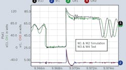
Most of the power loss occurs in this resistor. The turn-off time of a diode is determined by the time required to remove its stored charge, possibly less than trr. For an R2CD snubber, if the half period of resonance is small compared to trr, then the diode turns off with no switching transient. As trr increases, there is no penalty, mitigating the dearth of specifications for these diodes. It’s especially noteworthy that EMI generated by the switching transient of a properly designed R2CD snubber is actually less than the RCD version. Fig. 4 shows the simulation waveforms illustrating how the R2CD snubber works.
Fig. 4. The R2CD snubber (red and green traces) produces less EMI than the RCD snubber.
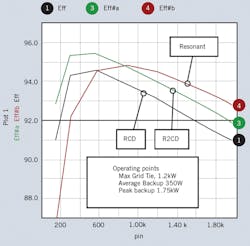
Three snubber configurations have been compared using a kilowatt level full bridge DC-DC converter. The output bridge drives a buck type L-C filter in a manner that produces a 120 VRMS full wave rectified sine wave. The input bridge is connected to a combination 48 Volt battery and solar panel battery charger. Bi-directional power conversion is required so that motor loads can be supplied as well as battery charging. Normally all transistors in the output bridge are turned on so that the load current flows through the transformer secondary. When power is needed, opposite output bridge switches are turned off and corresponding input bridge switches connect to the battery/charger system. Thus, the initially charged transformer leakage inductance must be discharged into a snubber. In this case, the snubber protects the high-side driver components because the switches are avalanche rated.
The RCD and R2CD snubbers are the same ones evaluated in the test simulation. A resonant snubber based on [2] was included in the evaluation. Fig. 5 shows the results.
Fig. 5. R2CD snubber has best overall efficiency below 1 kW.
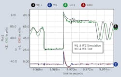
Additional simulation and tests were run on a two Watt housekeeping power supply and are summarized in Fig. 6.
Fig. 6. Two Watt R2CD snubber simulation compares favorably with lab test results.
The simulation parameters were adjusted to match the test results. VR1 is the voltage across snubber resistor R1. The major adjustments were for leakage inductance (adjusted in the transformer model by changing the insulation thickness) and varying diode trr.
Discussion
Simulation Vs. Test: It is important to make test and simulation results agree. Once the simulation results match the test results; then simulation parameters can be varied in order to evaluate circuit performance for varying tolerances and temperatures. Some of these
parameters; trr for example, can’t be varied by part substitution. The equations describing snubber loss are approximate and don’t include the complex behavior of switched current, voltage and time. So like it or not, simulation is a required design tool!
RR2CD Topology: Variations in the R2CD topology yield the same results. These variations include moving R1 to be anywhere in series with C; for example on either side of the diode, the ground leg or in series with C. Similarly, R can go anywhere after the snubber diode. Placing R1 in the ground leg simplifies measuring snubber current. C can be connected to ground or the output. Connecting to the output increases conducted EMI and reduces the required voltage rating.
Leakage Inductance: The power to be snubbed is,
so that minimizing leakage inductance is the first priority. Leakage inductance is difficult to predict [1] because magnetic device geometry depends on winding techniques, Therefore, is necessary to measure leakage inductance by shorting out the secondary windings. Measuring leakage inductance is surprisingly more complex than it appears. Consider an equivalent circuit where magnetizing inductance is in parallel with a series combination of leakage inductance and reflected winding resistance. An LCR mulltimeter will report vastly different results at 1 kHz vs. 100 kHz. For the circuit used in
Fig. 5, the result is 168 µH vs. 5 µH. In any event, the short circuit driving point impedance needs to be compared to the simulation result in order to evaluate or adjust the transformer model.
EMI reduction: The reduced EMI is caused by the resonant charge characteristics (Fig. 2). To get the best result R1 must be set based on L and C (Equation 1) so that the only degree of freedom in the design is the selection of C. As C increases, voltage clamping is reduced but efficiency is reduced. R1 can be cut in half (k = 1 in Equation 1) without much change in the EMI characteristic in order to reduce the maximum voltage.
Efficiency: To calculate the RCD snubber power loss; First, Calculate the power loss in a Zener clamped snubber with no switch capacitance:
Then replace the zener with a resistor having the same average current.
Where:
VM = Maximum or snubbed voltage
Vs = Input voltage
nVs = Flyback voltage
F = Frequency
L = Leakage inductance
Is = Switched current
PZ = Zener power
PR = Resistor power
The R2CD snubber loss is just PL, so the RCD snubber is flawed by not having available the proper voltage, nVs, to connect the bleed resistor.
Some of the energy of the switched leakage inductance is dissipated in the switching transistor. The R2CD configuration dissipates less of this energy in the switching transistor. Actual values depend on the transistor, its drive circuit and the direction of power flow.
For the R2CD snubber, R is used to control the final value of charge. Simulation can be used to find a value for R that minimizes EMI.
Diode Selection: The R2CD snubber diode relies on unspecified data sheet parameters. Two important parameters are storage time and the forward recovery characteristic [4]. Forward recovery occurs when the diode is switched on because of the low initial conductivity of the intrinsic region. For the R2CD snubber, the initial turn-on resistance, Rm, can be used as a figure of merit. Table 2 lists the characteristics and cost for several common diodes. Rm and energy were based on test using a 5 A current pulse. Multiplying energy by operating frequency gives the power dissipation caused by forward recovery. The loss is expected to grow proportional to the square of current. Detailed test data is available [3].
The 1n4007 used three devices in parallel and cost data for 500 quantities. All others used 100 quantities for pricing. Digi-Key was used for the price estimates. All trr values were in the acceptable range for the application. Notice the newer, “modern” technology diode had greater
forward recovery loss and costs more. The 20ETS12 data was representative of 2 other part numbers (40EPS08 and D6020L) that were even more expensive. For reference, the DSEP8-12A fast recovery diode used in an RCD snubber costs $1.37.
Test Circuit: The circuit in Fig. 2 simulates snubber loss so that testing can be accomplished at lower power. The actual circuit (Buck or Flyback) operates at much higher power.
Conclusion
The simulation results speak loudly! The R2CD snubber is more efficient, lower cost and produces less EMI. The popular misconception that diode storage time must equal the resonant ½ period is replaced by the requirement that storage time be greater than the resonant
1/2 period. More hardware tests are available along with the production and test drawings [3]. The R2CD snubber is surprisingly immune to circuit parameter variation; while limiting peak voltages for wide variations in R1, R, C and trr.
References
[1] Magnetics Designer Manual. Published by Intusoft, available in PDF format from
http://www.intusoft.com/lit/Magdes.pdf pg 157
[2} L.G. Meares, “Improved Non-Dissipative Snubbers for Buck Regulators and Current-Fed
Inverters”, Proceedings of Powercon 9, July 1982, pp B-2,1-8.
[3] http://www.intusoft.com/snubbetTest.htm
[4] Cliff L. Ma and P.O. Lauritzen “A Simple Power Diode Model with Forward and Reverse
Recovery”. IEEE Transactions on Power Electronics, vol 8, No.4, October 1993.
