Why SiC Devices?
Silicon Carbide (SiC) MOSFETs exhibit higher blocking voltage, lower on state resistance and higher thermal conductivity than their silicon counterparts. SiC MOSFETs are designed and essentially processed the same way as silicon MOSFETs. The enhanced performance is derived from the material advantages inherent in the silicon carbide physics. Due to its simple structure, ease of a design-in, and low drive losses, the N-channel enhancement mode SiC MOSFET offers good compatibility as a replacement for silicon MOSFETs and IGBTs.
Related Articles
- SiC and GaN Vie for Slice of the Electric Vehicle Pie
- 1200V SiC MOSFET Poised to Replace Si MOSFETs and IGBTs
- SiC "Super" Junction Transistors Offer Breakthrough High Temp Performance
- SiC: A Rugged Power Semiconductor Compound To Be Reckoned With
- Design Considerations for SiC-based Power Electronics
- Test Equipment Must Keep Pace with New High Power Semiconductor Developments
What nomenclature do SiC devices employ? SiC transistors borrowed the same nomenclature as their silicon brethren: gate, drain and source, as shown in Fig. 1. In addition, on-resistance and breakdown voltage of a SiC device have a similar meaning as their silicon counterparts. On-resistance (RDS(ON)) vs. gate-source voltage curves are similar to silicon MOSFETs. The temperature coefficient of SiC MOSFET on-resistance is similar to the silicon MOSFET as it is positive, but the magnitude of RDSon change is less over the device operating range.
SiC Transistor History
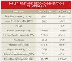
How has the SiC transistor evolved? Adoption of SiC semiconductors has been limited by substrate costs, the material’s physical idiosyncrasies and defect density. These issues have limited SiC devices to diodes in the last five years. However, the wafer processing challenges have been largely resolved with development of low-defect SiC wafers that make it possible to produce SiC MOSFETs. Cree introduced the first SiC MOSFET in January 2011. This CMF20120D transistor was rated at 1200V, had 80 mΩ on-resistance, and was housed in TO-247 package. Although its cost was higher than the Si IGBT it was supposed to replace, the SiC MOSFETs have faster switching, better efficiency and better thermal performance. The second generation SiC MOSFET, C2M0080120D, was released in March 2013 and has improved performance characteristics. Table 1 compares the key device parameters of the first and second generation parts. Note, in particular, the reduction in die size and associated capacitance values. This contributes to the better switching efficiency of the Gen2 device and the sizable cost reduction as well.
Power Modules
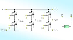
Are there any SiC MOSFET Power Modules? Cree introduced the industry's first commercially available all-silicon carbide (SiC) six-pack power module in an industry standard 45 mm package (Fig. 2). When replacing a silicon module with equivalent ratings, Cree's six-pack module reduces power losses by 75 percent, which leads to an immediate 70 percent reduction in the size of the heat sink, or a 50 percent increase in power density. The six-pack SiC module unlocks the traditional design constraints associated with power density, efficiency and cost, thereby enabling the designer to create high performance, reliable and low cost power conversion systems. When compared to state-of-the-art silicon modules, the SiC 1.2 kV, 50 A modules deliver performance equivalent to silicon IGBT modules rated up to 150 A depending upon efficiency requirement and switching frequency.
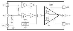
What gate drivers can be used with a SiC MOSFET? Gate driver ICs suitable for SiC MOSFETs are available from IXYS, Texas Instruments and most recently from Avago. Texas Instruments’ UCC2753x IC family are single-channel, high-speed, gate drivers capable of driving SiC MOSFET power switches by up to 2.5 A source and 5 A sink (asymmetrical drive) peak current (Fig. 3). Strong sink capability in asymmetrical drive boosts immunity against parasitic Miller turn-on effect. The UCC2753x can also feature a split-output configuration that allows the designer to apply independent turn-on and turn-off resistors to the OUTH and OUTL pins, respectively, and easily control the switching slew rates.
The driver has rail-to-rail drive capability and extremely small propagation delay, typically 17 ns. The input threshold of UCC2753xDBV is based on TTL and CMOS compatible low-voltage logic, which is fixed and independent of VDD supply voltage. Its 1V typical hysteresis offers excellent noise immunity.
IXYS’ IXD_609SI is an automotive grade, high-speed gate driver. Its output can source and sink 9 A of peak current, while producing rise and fall times of less than 45 ns. Both the output and input are rated to 35 V. The input is virtually immune to latch-up, and proprietary circuitry eliminates cross conduction and "shoot-through." The IXD_609SI has a Grade 1, -40 °C to +125 °C ambient operating temperature range. It is AEC Q100 qualified and available in an 8-pin Power SOIC package with an exposed metal back.
Avago’s ACPL-P346 is a high-speed 2.5 A gate drive optocoupler that contains an AlGaAs LED, which is optically coupled to an integrated circuit with a power output stage. This optocoupler is ideally suited for driving power and SiC MOSFETs used in inverter or AC-DC/DC-DC converter applications. The high operating voltage range of the output stage provides the drive voltages required by gate controlled devices. The voltage and high peak output current supplied by this optocoupler make it ideally suited for direct driving MOSFETs at high frequency for high efficiency conversion. The ACPL-P346 has the highest insulation voltage of VIORM= 891 V peak in the IEC/ EN/DIN EN 60747-5-5 and is UL1577 recognized with 3750 VRMS for 1 minute.
Optimizing Layout
How do you optimize layout to ensure proper gate drive? To achieve fast switching time, the gate drive interconnections must have minimum parasitics, especially inductance. This requires the gate driver to be located as close as possible to the C2M0080120DD. Exercise care in selecting an appropriate external gate resistor to manage voltage overshoot and ringing. As with any majority carrier device, the C2M0080120D has no tail, so the amount of drain voltage overshoot and parasitic ringing is noticeably higher. The higher ringing can be a concern, because the lower transconductance and low threshold voltage of the C2M0080120D di/dt can couple back to the gate circuit through any common gate/source inductance. Ferrite beads help minimize ringing while maintaining fast switching time. A high value resistor (10 kΩ) between gate and source should be used in order to prevent excessive floating of the gate during system power up propagation delays.
Does the SiC MOSFET have a body diode? Like conventional silicon MOSFETs, the SiC MOSFET has a body diode – a PN type with 3.1 V to 3.3 V threshold voltage. The higher turn-on voltage reduces efficiency slightly versus an external SiC Schottky diode, but the body diode has a much lower reverse recovery charge than a silicon MOSFET’s body diode.
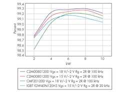
How does the efficiency of the two generations of SiC MOSFETs compare with silicon IGBTs? Fig. 4 shows efficiency testing data with the SiC MOSFETs at 100KHz (first generation SiC MOSFET CMF20120D and second generation SiC MOSFET C2M0080120D) and Si IGBT (IGW40N120H3) at 20 KHz. Output diodes used for both switch devices were Cree 1200 V SiC Schottky diode C4D10120D, thus assuring a fair comparison. All data are based on an external gate resistor of 2 Ω. Even with five times the switching frequency, the SiC solution was able to achieve a maximum efficiency of 99.3% at 100 KHz, reducing losses by 18% from the best efficiency of the IGBT solution at 20 KHz. At light loads, where the two designs exhibit the poorest efficiency, the 100 KHz SiC solution still matched the 20KHz performance of the silicon system. This comparison shows that the SiC MOSFET exhibits both an efficiency and a frequency advantage over a silicon IGBT. Highly efficient systems can thus be designed with SiC MOSFETs at switching frequencies that allow lower magnetic element values, reducing overall system size, weight and cost.
Minimizing EMI
What should be done to minimize EMI in SiC MOSFET circuits? EMI design should be given attention with high frequency SiC power devices. There are some practical approaches that can be employed to limit the influence of noise with high switching frequency. With high switching frequency and fast switching times of SiC MOSFETs, drain voltage ringing is potentially much higher due to parasitic oscillation, especially due to parasitic capacitance of the inductor. When the circuit switches are turn-on and turn-off, there is high frequency resonance between the parasitic capacitance of inductor and stray inductance in the switching power loop, which will lead to excessive ringing. To reduce the ringing at high frequency, use a single layer winding inductor. A single layer winding can dramatically reduce the parasitic capacitance of the inductor with good flux coupling. The will result in reduced ringing within the VDS switching node.
This article was prepared with the help of Cree Inc., Durham, NC.


