Leadless MOSFET Power Package Achieves Near-GaN Switching Losses
Newly available SMD power semiconductors support fast switching and reduce the parasitic inductance associated with the long leads on packages like the TO‑220 or TO‑247. However, the thermal management challenge is historically difficult using SMDs.
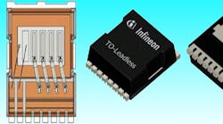
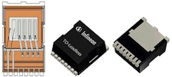
This is particularly true in high-power PFC (power factor correction) circuits and it is the main reason that TO‑220 and TO‑247 packages are still preferred by many engineers for this type of application. Now, newly available TO-LeadLess (TOLL) packages (Fig. 1) matched with latest-generation superjunction MOSFET technology, offer the opportunity to migrate even high-power PFC circuits to SMD solutions.
It is also important to consider improvements in packaging to deliver real-world application benefits. This is where the TOLL package comes in. TOLL is a recently developed SMD package optimized for high-power, high-voltage, and high-reliability applications. While new, it benefits from experience with low- and medium-voltage versions that are already successfully used in a variety of industrial and automotive applications.
The small size of the TOLL package is ideal for modern, dense SMPS designs where high current capability combined with low thermal resistance (RTHJC) results in less waste heat. This allows designers to develop more efficient systems. And because TOLL devices have no leads, parasitics that counteract the drive voltage and reduce efficiency in leaded packages such as TO‑247 can be eliminated.
CoolMOS G7
Packaging is important in Infineon Technologies’ CoolMOS process, a proven technology that has benefitted from substantial development since the introduction of its novel drain structure in 1999. The inherent quality of this mature technology is illustrated by the fact that in the last 1.6 billion CoolMOS units shipped, there have only been 38 failures.
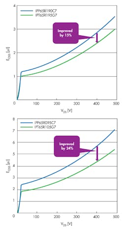
The G7 silicon technology is an enhancement of the 650 V CoolMOS C7 that superseded CoolMOS CP in early 2013. One of its major features is the reduction of Eoss. For hard switching applications (such as PFC) this energy is converted into heat each time the device is turned on with a positive gate signal and becomes wasted energy.
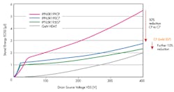
As shown in Fig. 2, G7 achieves a15 % reduction in EOSS (the energy stored in the output capacitance) compared to C7, which in itself had achieved a 50% reduction compared to earlier technology. Figure 3 shows EOSS improvements with the C7 process.
At just 33 mΩ, MOSFETs in the new device family offer the lowest available RDS(ON) for any 650 V SMD device. This makes them ideal for high-power, hard-switching PFC as well as low switching and conduction-loss-dominated bridge-rectifier replacement.
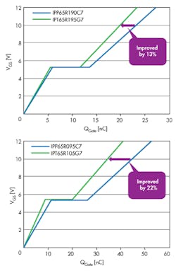
Although lower QG delivers lower gate driving losses, QGD has a significant impact on switching transition times and losses. Figure 4 shows the gate-charge comparison between 650 V CoolMOS C7 and G7 based on the 195 mΩ and 105 mΩ devices. It should be noted that it is not possible to compare the 33 mΩ device as there are no comparable devices available.
It is very clear from the graphs that the new technology offers approximately 15‑20% lower gate charge and will therefore switch faster with significantly lower switching losses, thus providing the performance that modern power designs require.
To illustrate the impact of this, the switching losses of the CoolMOS G7 are reduced such that a 105 mΩ device exhibits the same switching losses as a 125 mΩ device from the previous technology generation. It is now possible to use (for the same power range) the lower RDS(ON) device in order to reduce the overall power losses while retaining the same light load efficiency.
There are also advantages when it comes to manufacturing. The totally Pb‑free package has an MSL1 rating for easy handling on the shop floor and is compatible with both wave and reflow soldering, facilitating high levels of flexibility. Moreover, the tin‑plated leads feature a trapezoidal groove next to the PCB pad. This guarantees wetting and means that the joint is fully visible for optical inspection systems, ensuring the quality of the finished product.
CoolMOS G7 in TOLL packaging
Bringing together 650 V CoolMOS G7 with TOLL packaging delivers, literally, a very powerful combination of technologies for power-supply designers. The advantages of this generation of MOSFETs will make a significant contribution to leading-edge power-supply design. However, the semiconductor technology is just one part of the story.
The enhanced MOSFET technology reduces the switching losses, so it can be used at higher switching frequencies. This allows reduced size of the magnetic components, which in turn enables reduced form factors and lower overall costs.
The TOLL SMD package offers 4‑pin Kelvin Source functionality in order to optimize the switching behavior. The lowest RDS(ON) offered in the TOLL package is 33 mΩ compared to previous best-in-class C7 technology of 45 mΩ in the TO‑220 or D2PAK.
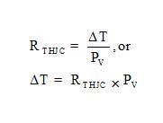
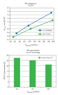
Thermal resistance (RTHJC) of the device is a very important measure of the cooling performance. CoolMOS G7 devices offer a 20% improvement for the same RDS(ON) when compared to conventional packages such as D2PAK. RTHJC, thermal resistance junction-to-case, is an important power semiconductor characteristic that is described in:
Where:
DT = Temperature difference in °C
PV = Power in watts
The RTHJC improvement results in lower silicon temperatures for the same level of heat transfer or power losses. Figure 5 shows the normalized improvement as a percentage based upon interpolated RDS(ON) for the new devices compared to the previous generation baseline. This results in lower values because RDS(ON) significantly increases with device temperature.
Lowering operating temperatures provides engineers with significantly enhanced design flexibility. They can choose to reduce the cooling or increase the power output, either of which would increase power density. If no changes are made the reliability is increased as the system runs at a lower temperature.
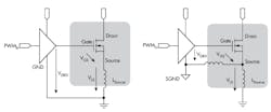
The TOLL package also offers a Kelvin Source connection that reduces the parasitic source inductance being fed back to the gate voltage, resulting in both faster switching and cleaner gate waveforms. Figure 6 compares the standard gate-drive scheme and the 4-pin approach that utilizes the Kelvin Source.
The TOLL package also has very low parasitic inductance (approximately 1 nH) when compared with the TO247 package (~15 nH). Thus, the bouncing of the signal ground is much lower, which reduces the voltage peaks at transition.
With its ability to reduce losses, G7 represents the state-of-the-art in terms of superjunction MOSFET technology, while the TOLL package brings benefits in terms of size, thermal performance and reduced parasitics. When combined, G7 and TOLL give engineers significant benefits and options in designing high-density, highly efficient power systems.
