On-Chip MCU Supervises Operation Of Power Conversion Controller IC
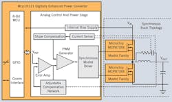
Using traditional analog control circuits, the MCP19111 from Microchip Technology regulates the output of a synchronous, step-down dc/dc converter with a 4.5 to 32 V input range). Also on-chip is a version of Microchip’s PIC® MCU mid-range core that enables customization of device operating parameters, start-up and shut down profiles, protection levels and fault handling procedures. The MCP19111 (Fig. 1.) MCU is housed in a space-saving, 28-pin, 5 mm x 5mm QFN package with integrated synchronous drivers, an internal linear regulator, and 4 kW flash memory. To complete a full-fledged power management system, Microchip developed a high-speed MOSFET family, optimized specifically for use with the MCP19111. The family includes the MCP87018, MCP87030, MCP87090 and MCP87130. They are 25 V-rated, 1.8 mΩ, 3 mΩ, 9 mΩ and 13 mΩ logic-level MOSFETs. MCP87030 and MCP87018 MOSFETs are offered in a 5x6 mm, 8-pin PDFN package. The MCP87090 and MCP87130 MOSFETs are offered in both a 5x6 mm, 8-pin PDFN package, as well as a 3.3x3.3 mm, 8-pin PDFN package
Fig. 1. Block diagram of the MCP19111 shows the integrated MCU and controller IC.
Digitally-controlled supervision of power management allows MCU register settings to configure the device, rather than adding or modifying external hardware. The MP19111’s low power, 8-bit MCU easily performs all necessary supervisory functions. Supervision programmability permits the designer to optimize efficiency, protect the analog section, provide 15 general purpose I/O connections, and include some established PMBus instructions using an I2C interface.
Internal Power
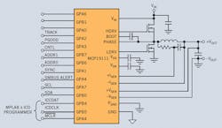
Fig. 2 shows a typical application for the MCP19111, which has two internal linear regulators that generate 5 V rails. One is an on-chip 5 V rail that powers internal analog circuits. Located at the VDD pin is a second 5 V rail that powers the MCU.
Fig. 2. Typical MCP19111 application drives two external synchronous MOSFETs .
The internal gate drivers can drive two external N-Channel MOSFETs in a synchronous buck topology. The gate of the floating MOSFET is connected to the HDRV pin. The source of this MOSFET is connected to the PHASE pin. The HDRV pin source and sink current is configurable. Setting a bit in an internal register allows the high-side to source and sink 1 A peak current. By clearing this bit, the source and sink peak current is 2 A.
The low-side MOSFET gate connects to the LDRV pin and the source of this MOSFET connects to PGND. The drive strength of the LDRV pin is not configurable. This pin can source 2 A of peak current and peak sink current is 4 A. This helps keep the low-side MOSFET off when the high-side MOSFET turns on.
Current required to drive the external MOSFETs is:
IDRIVE = [QG(High) + QG(LOW)] ×FSW (2)
Where:
IDRIVE = Drive current in A
QG(HIGH) = Total gate charge of the high-side MOSFET in nC
QG(LOW) = Total gate charge of the low-side MOSFET in nC
FSW = Switching frequency in MHz
Synchronous MOSFET dead time occurs when one drive signal goes low and the complimentary drive signal goes high. The MCP19111 can adjust both the high-side and low-side driver dead times independently by using register settings that enable 4 ns increments.
The MCP19111 can disable the entire synchronous driver or just one side of the synchronous drive signal. A register setting disables the entire synchronous driver when the HDRV and LDRV signals are set low and the PHASE pin floats. Clearing the disable bit allows normal operation.
Register settings also configure the output voltage, eliminating the need for an external resistor divider to set the output voltage. Plus, the MCP19111 contains a unity gain differential amplifier used for remote sensing of the output voltage. Connecting the amplifier’s +VSEN and
-VSEN pins directly at the load allows better load regulation.
You can configure the switching frequency from 100 kHz to 1.6 MHz. A timer module generates the HDRV/LDRV switching frequency. Typically, the MCP19111 is set to a 300 kHz switching frequency.
Compensation
A register setting adjusts the controller IC’s compensation zero frequency and gain. Fig. 3 shows the internal compensation network with the output differential amplifier showing the +VSEN and –VSEN pins.
Fig. 3. Internal compensation network with the output differential amplifier.
In current mode control systems, slope compensation must be added to the PWM circuit to prevent subharmonic oscillation when operating with duty cycles greater than 50%. The MCP19111 adds a negative slope to the error amplifier output signal before it is compared to the current sense signal. The amount of slope added is controlled by a register.
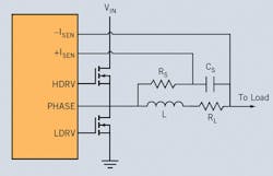
Output current sensing can use either a resistor placed in series with the output, or the series resistance of the inductor. Using an inductor series resistance requires a filter to remove the large AC component of the voltage that appears across the inductor and leave only the small AC voltage that appears across the inductor resistance. This small AC voltage is representative of the output current. Fig. 4 shows the inductor current sense filter.
Fig. 4. Current filter removes the AC component of the inductor voltage.
You can find RS and CS from:
Where:
L = Inductance of the output inductor in henries
RL = Series resistance of the output inductor in ohms
RS = Current sense filter resistor in ohms
CS = Current sense filter capacitor
When the current sense filter time constant is set equal to the inductor time constant, the voltage appearing across CS approximates the current flowing in the inductor multiplied by the inductance.
Protection Features
An Analog-to-Digital Converter (ADC) allows conversion of an analog input signal to its 10-bit binary representation. The ADC uses analog inputs, which are multiplexed into a single sample and hold circuit. The output of the sample and hold connects to the controller input. The controller generates a 10-bit binary result via successive approximation and stores the right justified conversion result in the ADC result registers.
You can monitor the output voltage measured between the +VSEN and -VSEN pins using the internal ADC. When this ADC reading matches a user-defined power good value (determined by firmware), it can toggle a GPIO (general purpose I/O) to indicate the system output voltage is within a specified range. You can use firmware to configure delays, hysteresis and time out values.
To facilitate system prototyping, various internal signals can be measured by configuring the MCP19111 in bench test mode. To accomplish this, the ATSTCON bit is set. This configures GPA0 as the ANALOG_TEST feature. The signals measured on GPA0 are controlled by bits of the BUFFCON register. The ADC/multiplexer provides access to measurement of the internal analog signals.The MCP19111 features a hardware overtemperature shutdown protection set at +160°C typically. No firmware fault-handling procedure is required to shutdown the MCP19111 for an overtemperature condition. Typically, if the internal temperature of the MCP19111 reaches +140°C the MCP19111 clears a register bit. This bit remains cleared until set by firmware.
Firmware can control soft start of the output voltage. Internal registers settings can produce very long soft start times.
You can configure the MCP19111 to track another voltage signal at start-up or shutdown. The ADC can read a GPIO that has the desired tracking voltage applied to it. Then, firmware compares the internal output voltage reference to this ADC reading.
Register settings and flags allow the designer to configure other MCP19111 functions, including:
- Input Under-Voltage Lockout
- Output Over-Current
- Current Sense AC Gain
- Output Compensation
- Slope Compensation
- Output Voltage Configuration
- Output Under-Voltage
- Output Over-Voltage
Analog Peripheral Control
You can configure various analog peripherals that enable customizable operation.
- Diode Emulation Mode
- High-Side Drive Strength
- MOSFET Driver Dead Time
- Output Voltage Sense Pull-Up/Pull-Down
- Output Under-Voltage Accelerator
- Output Over-Voltage Accelerator
Analog Blocks Enable Control
Using enable bits located in the ATSTCON register you can enable or disable various analog circuit blocks:
- Output Over-Voltage Enable
- Output Under-Voltage Enable
- Relative Efficiency Measurement Control
- Slope Compensation Control
- Current Measurement Control
- Internal Temperature Measurement Control
- Relative Efficiency Circuitry Control
- Signal Chain Control
Device Calibration
Calibration words are stored in flash program memory that is readable and writable during normal operation (full VIN range). This memory is not directly mapped in the register file space. Instead, it is indirectly addressed through the Special Function Registers used to read and write this memory. Read-only memory locations 2080h through 208Fh contain factory calibration data, including:
- Offset Calibration for The Output Voltage Remote Sense Differential Amplifier
- Overtemperature Shutdown Threshold
- Internal Bandgap Voltage Reference for the ADC
- Buffer Amplifier Offset of the Output Voltage Regulation Reference Set Point
- Error Amplifier Offset
- ADC Reading From The Internal Temperature Sensor
- Output Voltage Difference Amplifier Offset
- Unity Gain Buffer Offset Voltage
Memory Organization
There are two types of memory:
- Program Memory
- Data Memory
- Special Function Registers (SFRs)
- General Purpose RAM
The MCP19111 has a 13-bit program counter capable of addressing an 8K x 14 program memory space. Only the first 4K x 14 (0000h-0FFFh) is physically implemented. Addressing a location above this boundary will cause a wrap-around within the first 4K x 14 space.
Special Function Registers and peripheral functions control the MCU’s desired operation. These registers are static RAM.
The MCP19111 has a temperature measurement of silicon die the operating temperature The circuit's range of the operating temperature falls between -40°C and +125°C. The ADC reads the output voltage that is proportional to device temperature.
In the MCP19111, the PWM module generates the system clock, which controls the switching frequency and sets the maximum allowable duty cycle. The PWM module does not continuously adjust the duty cycle to control the output voltage. The analog control loop and associated circuitry performs the adjustment. However, this duty cycle cannot be greater than the value in the PWMRL register.
Instruction Set
The MCP19111 instruction set is highly orthogonal and has three basic categories:
- Byte-oriented operations
- Bit-oriented operations
- Literal and control operations
Each instruction is a 14-bit word divided into an opcode, which specifies the instruction type, and one or more operands, which further specify instruction operation. One instruction cycle consists of four oscillator periods. For a 4 MHz oscillator frequency this yields a normal instruction 1 μs execution time. All instructions execute within a single instruction cycle, unless a conditional test is true, or the program counter is changed as a result of an instruction. When this occurs, the execution takes two instruction cycles, the second cycle executes as a NOP.
MPLAB Integrated Development
A Graphical User Interface (GUI) aids in development of MCP19111 firmware. You can use this GUI to quickly configure the MCP19111 for basic operation. You can also add customized or proprietary features to the GUI-generated firmware. The MCP19111 also features firmware debug support.
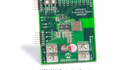
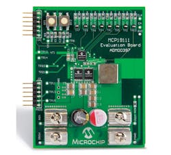
Also available is the MCP19111 Evaluation Board (ADM00397) that includes Microchip’s power MOSFETs (Fig. 5).
Fig. 5. The MCP19111 Evaluation Board includes Microchip’s power MOSFETs.
Offered with standard firmware, the evaluation board is user-configurable through the MPLAB® X IDE GUI plug-in. The combined evaluation board, GUI and firmware allow power-supply designers to configure and evaluate the performance of the MCP19111 for their target applications.
The MPLAB IDE software brings an ease of software development not usually seen with 8/16/32-bit MCU applications. MPLAB IDE supports multiple debugging tools in a single development paradigm, from the cost-effective simulators, through low-cost in-circuit debuggers, to full-featured emulators. This eliminates the learning curve when upgrading to tools with increased flexibility and power. The MPLAB IDE is a Windows® operating system-based application containing:
- A single graphical interface to all debugging tools
- Simulator
- Programmer (sold separately)
- In-Circuit Emulator (sold separately)
- In-Circuit Debugger (sold separately)
- A full-featured editor with color-coded context
- A multiple project manager
- Customizable data windows with direct edit of contents
- High-level source code debugging
- Mouse over variable inspection
- Drag and drop variables from source to watch windows
- Extensive on-line help
- Integration of select third party tools, such as IAR C Compilers
The MPLAB IDE allows you to:
- Edit your source files (either C or assembly)
- One-touch compile or assemble, and download to emulator and simulator tools (automatically updates all project information)
- Debug using:
- Source files (C or assembly)
- Mixed C and assembly
- Machine code
