Customized Power Management ICs Compete with Standard Types
One approach to power management design is to integrate the necessary functions into what is called an iASIC, or integrated ASIC. This might yield a lower cost single chip solution while retaining all the desired power saving functionality of the original designs. You may be able to produce an iASIC (a chip integrating existing functions without the need to create new IP) in a relatively short development time.
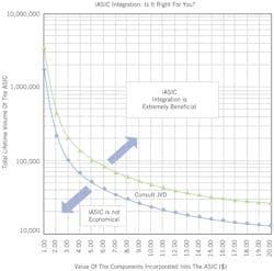
The iASIC approach may not be for everyone. Fig. 1 shows the financial economic benefits of integration using an iASIC.
Fig. 1.The iASIC approach may not be for everyone, particularly at low volume production.
Power Management is more than developing solutions that run cool and conserve power. It’s also about managing cost. Financial management is inextricably intertwined with power management. Often power management solutions transcend multiple product generations. It’s one place to drive cost out of a system for greater long term savings.
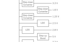
Fig. 2 represents the power board for a typical consumer application. Depending on total volume, the Bill of Materials may range from $1.00-$1.50 at the low end, to perhaps as high as $2.00.
Fig. 2.Power board circuit for a typical consumer application.
Using the iASIC technique, the IC could look like Fig. 3. The cost of the iASIC for the above set of requirements would be in the neighborhood of $0.60 each.
Fig. 3.Using the iASIC, the IC in Fig. 2 could look like this.
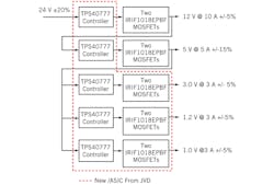
Fig. 4.Power management circuit design using five controllers and 10 power MOSFETs.
The BOM cost can be high, even in high volume. By selectively choosing to integrate six MOSFETs into the iASIC design along with the five controllers as shown in Fig. 5 outlined in red, the part count can be reduced from 15 to 5 and the cost of the iASIC would be approximately $1.50.
Fig 5.iASIC design for the circuit in Fig. 4.
Every design is created, transistor- by-transistor. You can target fully customized designs at various Bipolar, CMOS, and BiCMOS processes, guaranteeing the best cost/per formance match for the application.
Step 1: Specification Agreement
Customers meet with JVD engineers to review the requirements of the application. Design methodologies are discussed, including those that will facilitate the successful testing of the final chip. When the specification is completed, including functional blocks, pin-outs, packaging, process requirements, and critical performance parameters, a quotation is made that then forms the basis for a development contract.
Step 2: Design and Verification
To minimize risk, the latest analog simulation and verification tools from Cadence, OrCAD, PSpice, DW-2000, Altium are used. When possible, the critical aspects of the design are prototyped prior to releasing the design to layout. It is important to verify that the design performs correctly in a real application environment as well as through simulation. Upon completion of the design and verification phases, a review is held to determine proper performance.
Design approval allows a move to the layout phase.
Step 3: IC Layout
At this stage, any special ESD cells required by the design are generated as well as any unique I/O structures. Mixed signal and analog layout is tricky and best managed by hand to ensure optimal circuit performance and packing density. When the layout is complete, the device signal chain analysis is simulated under different process, temperature and voltage parameters, with particular attention paid to noise, capacitance, and parasitics. When approved at a second review, a GDSII “tape” is generated for the mask production.
Step 4: Mask Generation
Mask generation typically takes place at the silicon foundry. A mixed signal chip may have as many as 25 to 30 masks (photographic plates used in the process) An inspection of the masks is made by before they are released to the foundry.
Step 5: Manufacture Initial Samples
With the release of the masks, the foundry produces a batch of engineering prototype wafers - usually 6 to 12 wafers. Some wafers are retained for setting up probe and test in preparation for mass production. The others are processed into individual die and assembled into packages for ease of qualification of the part. The packages are then verified for operation in the specified application.
Step 6: Test Development
Although identified here as Step 6, test development is a parallel activity that begins at the same time as the design (Step 2), as it can take as long or longer to complete as the chip design itself. Test hardware and software must be at or near completion when the first prototype silicon arrives. Both the silicon and the automatic production tester undergo simultaneous debugging.
Step 7: Production
Once the initial samples have been qualified at the third and last review meeting, JVD prepares the tooling and probe test cards to manufacture and deliver production silicon.
Step 8: Lifetime Product Support
Throughout the product life, technical and manufacturing experts support the design and manufacturing requirements of the product. An inventory is maintained to ensure timely delivery of parts.


