Energy Harvesting Employs Low Quiescent Current, Multi-Mode PMIC
A power management integrated circuit (PMIC handles loads from microamps to hundreds of milliamps and can distribute power to devices employed in an energy harvesting system.
At the heart of an energy harvesting sensor system is the TPS65290 from Texas Instruments, a PMIC that provides efficient system management for loads ranging from fractions of a microamp to a few hundred miliamps. The IC operates over a 2.2 V to 5 V input range and incorporates:
1. Factory selectable low quiescent current always-on power supplies, including:
· 30 mA buck converter with 300 nA quiescent current
· 10 mA LDO with 400 nA quiescent current
· 10 mA Zero IDDQdrop with 100 nA quiescent current
2. 500 mA buck/boost converter employs PFM/PWM operation with forced PWM option
3. 150 mA low dropout regulator
4. Eight power distribution switches used to support different configurations for the various loads
Related Articles
- Efficient Boost Charger IC for Nano Power Energy Harvesting
- New energy manager IC for nanopower energy harvesting apps
- Energy-harvesting IC enables super-skinny applications
- Harvest time near for energy ICs
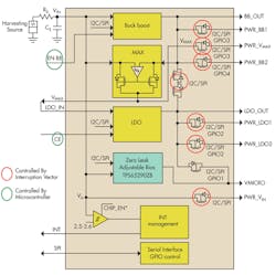
For energy harvesting applications, an integrated programmable input voltage monitor allows connection and disconnection of the different power blocks and switches without intervention of the master processor.
Choice Of Interfaces
To maximize control flexibility, the TPS65290 includes a factory-selectable choice between SPI and I2C interfaces. To minimize PC board footprint and reduce bill of materials (BOM) components and cost, the PMIC internally includes resistive dividers (boost/buck, LDO, VIN monitor); I2C pull-up resistors; SPI pull-down resistors; boost/buck compensation; and interrupt pull-up resistor. Only low-cost ceramic capacitors and power inductors are needed to complete a comprehensive multi-rail solution for efficient long-term data-acquisition systems.
The chosen serial interface for the part is SPI as I2C lines are open drain lines with internal 20 kΩ pull-up resistors that guarantee 400 kHz operation, but also create power losses when any of the bus lines are low. It is expected that operation with SPI will produce less average current consumption than I2C.
Applying a voltage higher than 1.95 V to VINcauses the always-on supply to start according to the factory default setting. This will be the only block available within the IC and will always stay on as long as the input supply does not drop below 1.95 V.
There are three possible choices for the always-on supply. The main parameter for choice is the “efficiency” of the supply during sleep mode, which is mostly processor current.
1. Zero Bias set to VIN-1.4
· Takes the least amount of quiescent current
· Provides voltage drops from 0.6 to 2 V in 200 mV steps
· Is not a regulated output
· Can be programmed to zero drop or to open circuit
· 10 mA max
2. LDOMINIset to 1.95 V
· Provides a regulated output
· Can be programmed from 1.8 to 3.3 V in 100 mV steps
· 10 mA max
3. BUCKMINIset to 1.95 V
· Provides a regulated output
· Can be programmed from 1.8 to 3.3 V in 100 mV steps
· 30 mA max
· Output has a ripple content
· Requires additional inductor (0603) and resistor (0402) PWR_AUX2 switch is disabled (pin becomes switching node)
Energy Harvesting Application
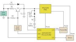
The TPS65290 can be used with low power, high impedance sources like those used in energy harvesting applications. As long as the input supply is higher than 1.95 V, the device will be fully operational and the serial interface can run with a clock as fast as 5 MHz. Fig. 1 shows the basic configuration where the current sourced by the harvesting supply is applied to a storage capacitor that provides the bulk of energy required by the system powered by the TPS65290.
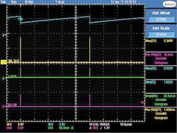
Fig. 2 shows the waveforms for basic system operation. A programmable rise/fall voltage comparator monitors the input supply (blue trace). Once the input reaches the rising threshold voltage the IC automatically enables switches that provide power to the different loads. Fig. 2 shows the enabling of the buck-boost regulator and the powering of its load, that makes the input voltage collapse. Once it reaches a preset falling edge threshold it generates an interruption and the switches can be disabled, effectively disconnecting the system loads. The associated micrcocontroller controls the enable and disable functions for the LDO and buck-boost.
Ideal for use within energy harvesting systems, TI’s ultra-low power MSP430FR5969 microcontroller can be efficiently powered by the TPS65290 device. Featuring a powerful 16-bit RISC CPU, which was specifically architected with ultra-low energy operation in mind, the MSP430FR5969 contains:
· Up to 64kB FRAM (FRAM is a new nonvolatile memory that combines the speed, flexibility, and endurance of SRAM with the stability and reliability of flash, all at lower total power consumption.)
· 2 kB SRAM
· 32-bit HW Multiplier
· HW Real Time Clock module
· Five 16-bit timers with multiple capture compare registers
· AES256 encryption /decryption accelerator
· Up to 3 serial communications channels
The MSP430FR5969 also includes ultra-low voltage analog peripheral modes that enhance its use in energy harvesting applications:
· 14 channel, 12-bit 200 KSPS ADC
· 16 channel analog comparator
· Temperature sensor
· Integrated precision voltage reference
Leveraging the latest developments in embedded memory, FRAM brings significant benefit to the energy harvesting market. Offering up to 250 times lower power operation compared to conventional flash-based MCUs, FRAM enables non-volatile data storage at µA rather than mA power levels. By integrating an AES hardware module, secure RF transmissions can be accomplished without the need for CPU intensive encryption / decryption algorithms, further extending system operating lifetime.
All operations, other than program-flow instructions, are performed as register operations in conjunction with seven addressing modes for source operand and four addressing modes for destination operand. The CPU is integrated with 16 registers that provide reduced instruction execution time. The register-to-register operation execution time is one cycle of the CPU clock.
The instruction set consists of the original 51 instructions with three formats and seven address modes and additional instructions for the expanded address range. Each instruction can operate on word and byte data.
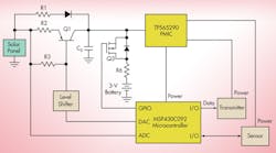
Shown in Fig. 3 is energy harvesting circuit with a rechargeable 3 V battery, solar panel harvesting source, and MSP430FR5969 ultra-low power FRAM microcontroller. R1 and R6 provide a direct path to power-up the TPS65290 and to maintain the energy storage process, even when disabling the TPS65290. Powering the MSP430FR5969 allows it to use its ADC to monitor the cell voltage and its DAC to control a current source (Q1, R2, R3) that extracts the maximum energy from the panel and stores it in CS. You can use Q3 to re-charge the battery and use R6 to limit the current charging/discharging the battery.


