System-on-a-Chip IC Enables Power Bank To Extend Life Of Battery-Powered Devices
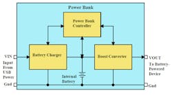
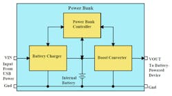
To understand the advantages of Active-Semi’s new ACT2800 family of Power Bank ICs, we have to look at a typical application. The Power Bank is essentially a battery in a sealed case used to supply power to a device whose battery has been exhausted. Usually, you connect a USB cable from a power source, such as a laptop, to supply power to charge the Power Bank’s internal battery. Then, you take the charged up Power Bank and its cable, and use it to connect to a smartphone or similar device with a depleted battery. Thus, the Power Bank serves to recharge the battery in the device with a depleted battery. This requires the Power Bank to provide a means to control the charge on its internal battery and also control the output to the device whose battery is depleted. Fig. 1 shows a simplified Power Bank circuit.
In a typical Power Bank implementation the associated battery-powered device is a smartphone with a micro-USB connector for charging its battery. The power input to the Power Bank is provided through a micro-USB connector and the Power Bank output will also use a USB connector. To charge the Power Bank’s internal battery, you use a cable with USB at one end and a micro-USB on the other end. You plug this cable into a USB port on a computer and then plug the micro-USB connector into the Power Bank. When the Power Bank’s battery is fully charged, you use the same cable by plugging the USB connector into the output of the Power Bank and the micro-USB connector into the charging input of the smartphone.
It is also possible to simultaneously connect both USB cables (i.e. provide input power to Powerbank, as well as simultaneously connect and charge phone battery as well. ACT2801/2 provides a direct power path from input to output with programmable current limit while providing power to switching charger. The output has higher priority than battery charger if the programmed input current limit is reached.
Most of today’s Power Banks require multiple ICs and additional external components to provide the charging and battery management functions. The ACT2800 family’s ACT2801 and ACT2802 ICs reduce the system footprint and minimize design complexity, while leaving room for larger batteries and reducing total system cost.
The ACT2801 and ACT2802 are functionally similar with different power handling capability, as shown in Table 1. They are both space-saving and high-performance low-profile single-chip solutions for a switching charger, boost converter and LED indicators. Table 1 shows the differences between these ICs. A high frequency switching frequency allows small size external inductors and capacitors.The ACT2801 and ACT2802 are both complete battery charge and discharge power management solutions for applications using single-cell lithium-based backup battery packs. Both the ACT2801 and ACT2802 provide similar functions. They charge the battery with a full cycle of preconditioning, fast charge with constant current and constant voltage until end of charge. These battery chargers are thermally regulated at 110 °C with charge current foldback.
The boost converters in the ACT2801 and ACT2802 both step the internal battery voltage up to a maximum of 5 V, with a programmable adjustment to a lower voltage. They feature high efficiency, constant current regulation, short circuit protection and overvoltage protection.
Four external LEDs driven by a 3.5 mA constant current source are used to indicate battery level and charge status for the ACT2801 and ACT2802.
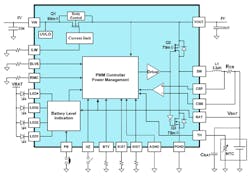
As shown in Fig. 2, the ACT2801 has a bi-directional architecture featuring a synchronous buck/boost converter you can configure as either a buck to charge the battery, or a boost to charge the external battery-powered device. This architecture allows higher charge current and higher conversion efficiency than traditional charge/discharge circuits.
The ACT2802 has a similar architecture with the primary difference of lower on-resistance for its internal power MOSFETs, as shown in Table 1.
Modes of Operation
The ACT2801/2 has three operation modes:
- Charge
- Boost
- High-impedance (HZ)
The charge mode enables the input current limit and configures Q2 and Q3 operate as a buck converter to charge battery. In the boost mode, MOSFETs Q2 and Q3 operate as boost converter to step up the battery voltage at VOUT, with current limit switch MOSFET Q1 turned off. MOSFET body diodes block leakage current from VOUT to VIN. In the HZ mode, MOSFETs Q1, Q2, and Q3 switches are turned off so battery drain current is very low.
Transitions between boost mode and charge mode go through the HZ mode by turning off all the switches for 2 seconds before enabling the other mode.
Modes are determined by the HZ pin and VIN pin, as shown in Table 2. A valid VIN voltage forces the ACT2801/2 into the charge mode. Boost mode is enabled if the HZ pin is pulled low and VIN is not present or not valid. Setting HZ to 0, and pulling the external momentary push button switch connected to the PB pin low for more than 100 ms, enables the boost converter. You can disable an enabled boost converter by:
1. After releasing push button PB, pull PB low for more than 3 seconds.
2. Keep the boost converter output current below its light load threshold for 1.5 minutes.
3. Let battery voltage fall below the boost cut-off threshold.
Input Current Limit
The ACT2800 family ICs are configured in charge (buck) mode when VIN is valid. A new charging cycle begins with the precondition state, and operation continues until VBAT exceeds the precondition threshold voltage. When operating in precondition state, the cell is charged at a reduced current, 10% of the programmed maximum fast charge constant current. Once VBAT reaches the precondition threshold voltage the state machine jumps to the fast charge state.
Regulation loops in the ACT2800 ICs regulate either current or voltage as necessary to ensure fast and safe charging of the battery (CC/CV). In a normal charge cycle, this loop regulates the current to the value set by an external resistor at the ICST pin. Charging continues at this current until the battery cell voltage reaches the termination voltage. At this point the CV loop takes over, and charge current decreases as necessary to maintain charging at the termination voltage.
If the battery voltage is above preconditioning threshold, the buck converter charges the internal battery with constant current. In the fast charge state, the ACT2801/2 charges at the current set by an external resistor connected at the ICST pin (Fig. 2). During a normal charge cycle fast charge continues in Constant Current (CC) mode until the internal battery reaches the charge termination voltage, at which point the ACT2801/2 charges in top off state.
When the battery voltage approaches End of Charge (EOC) as set by the BTV pin, charge current decreases as charging continues. In the top off state, the cell is charged in the constant voltage (CV) mode. During a normal charging cycle charging proceeds until the charge current decreases below the EOC threshold, defined as 13% of ICST. When this happens, the ACT2801/2 state machine terminates the charge cycle and jumps to the EOC state.
When charge current decreases to 13% of set fast charge current, the buck converter goes into EOC mode and keeps monitoring the battery voltage.
Recharge
When the internal battery voltage drops 200 mV below the EOC voltage, the charger is reinitiated with constant current (CC) charge.
Four LEDs flash on and off and then show the charge status and the remained capacity level as shown in Table 2. LED status is based on battery voltage and operation modes. In the charge mode, when a battery is fully charged, flashing stops and all four LEDs stay on.
Voltage thresholds for the four LEDs are adjusted from the HZ mode during charging and discharging based on the compensated impedance. Those thresholds are programmed by a resistor connected from BLVS pin to AGND as shown in Fig. 2. As long as LED4 is set, all the other three LED thresholds are fixed.
External Components
- The following external components are employed, as shown in Fig. 2:
- Resistor from ILIM pin to AGND sets the input current limit that has built-in soft start and a current foldback control loop.
- Resistor from the ICST pin to AGND sets the battery fast charge current.
- Resistor from the IOST pin to AGND sets the boost output current.
- Resistor RIMC sets the battery impedance between 40 mΩ to 500 mΩ. A higher RIMC gives higher compensation voltage which is positively proportional to battery charge/discharge current.
- Resistor Rbtv connected from BTV pin to AGND sets battery charge termination voltage. The Rbtv value depends on the battery voltage rating. Use a 1% accuracy resistor for Rbtv.
- Use a 2.2 µH SMD inductor for the input side, and 22 µF x 2 ceramic capacitors for the battery output side.
Battery Temperature Monitoring
The ACT2801/2 continuously monitors the temperature of the remote device battery pack by sensing the resistance of its NTC thermistor, and it suspends charging if the battery pack temperature exceeds the safety limits. In a typical application, the TH pin is connected to the battery pack's thermistor input as shown in the Fig. 2. The ACT 2801/2 inject a 60 μA current to the TH pin into the thermistor, so that the thermistor resistance is monitored by comparing the voltage at TH with the internal VTHL and VTHH thresholds of 0.3V and 1.5 V, respectively. When VTH > VTHH or VTH < VTHL charging and the charge timers are suspended. When VTH returns to the normal range, charging and the charge timers resume.
PC Board Layout
When laying out the printed circuit board, use the following checklist to ensure proper IC operation.
1. Arrange the power components to reduce the AC loop size consisting of C1, VIN pin, C2,
SW pin and the Schottky diode.
2. Place input decoupling ceramic capacitor C1 (22µF) as close to VIN pin as possible. CIN is
connected to power GND with vias.
3. Use a copper ground plane for best heat dissipation and noise immunity.
4. Place CSP and CSN capacitor C6 (10 nF) close to CSP and CSN pin as possible, use Kevin
Sense from sense resistor R2 to CSP and CSN pins. Add 22 µF x 2 decoupling capacitor close to BAT pin.
5. Place the ceramic capacitor C2 and D1 as close to VOUT and PGND as possible, SW
goes under the C2 (recommend C2 to use 1206 size). The SW pad is a noisy switching node, so It should be isolated from the rest of circuit for good EMI and low noise operation.
6. Connect a thermal pad to ground plane through vias (use 4 X 4 pins with a 10 mil aperture). Connect the ground plane, PGND and AGND to a single point under the ACT2801 thermal pad.
7. To reduce EMI noise, use an RC snubber from SW to PGND and add a 0.75 A /10 V
Schottky across the VOUT and SW pins.


