Calibrated Mains Frequency Monitor Delivers High Accuracy
In industrial setups that use equipment such as induction motors, it is important to maintain the proper frequency because the motor’s speed is a function of the frequency. More elaborate and sensitive setups may use ac drives to maintain the motor speed. However, in many situations, the motor may be directly connected to the power source without a drive, in which case variations in power frequency directly impact the motor speed. Here, we will show how to use a Silego GreenPAK SLG46620 and a few external components to build a frequency-deviation monitor that signals an alert if the frequency deviates by a specified margin.
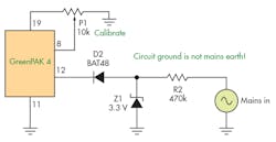
The design is based on measuring the period of the waveform. Many designs use a zero-crossing detector as the basis for period measurement. The mains input is stepped down and half-wave rectified with a few components (Fig. 1). The rectified pulses are fed to the GreenPAK chip and used to trigger an analog comparator (ACMP) reading at Pin 12.
The ACMP’s IN- terminal is held at 50 mV; when it toggles, it enables a counter that counts pulses from an internal oscillator until the end of the half-cycle. The ACMP’s low-bandwidth mode is enabled to prevent spurious responses due to noise. To determine whether the deviation of the mains-input frequency is acceptable, we use two digital comparators (DCMPs) to compare the counter’s output at the end of the half-cycle with two registers that store the upper and lower bounds we are interested in. DCMPs are available in the GreenPAK 4 series, and thus the SLG46620 was chosen for this circuit.
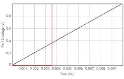
Figure 2 shows the first few microseconds of the half-wave cycle for a 230-V, 50-Hz waveform (black curve). The error introduced by using a half-wave rectifier in the manner stated above is quite small. Given the presence of the protective Schottky diode BAT48 at the input, we need a voltage of at most 350 mV to trigger the ACMP. The time taken for the mains voltage to reach a level of 350 mV is about 3.6 µs; double that to account for the ramp-down as well, and we have a 0.07% error that can be neglected in most mains frequency-monitoring applications. The red line in Fig. 2 represents the ACMP’s output.
Realization with the GreenPAK Designer
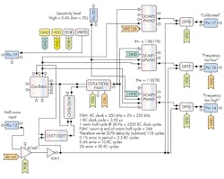
Figures 3 and 4 show the GreenPAK design. The broad idea is to drive the SET input of FSM1 low when the mains half-cycle starts, and bring it back high when the half-cycle ends. When the half-cycle ends, the rising edge produced by INV1 feeds into DFF6/7/8, locking the DCMPs’ states into pins 14, 16, and 17 respectively, after which the rising edge (delayed slightly by DLY7) sets FSM1.
To make the above strategy work in practice, we need to work around a couple of things. First, note that the GreenPAK 4’s DCMP works with 8-bit data, which offers a resolution of only 1 part in 256. What if we want better accuracy? Second, the internal oscillator is not as accurate as a crystal oscillator. Therefore, if we need to keep the external parts count really low, we need a method of calibrating the frequency monitor. This is discussed later in the article.
Oscillator and Counter Design
For the design, we chose a 2-MHz RC oscillator. The oscillator output divisor and the FSM1 clock input divisor are set to 2 and 4, respectively, so that the counter frequency is now 2000/8 = 250 kHz (period = 4 µs).
So, what happens with a nominal mains frequency of 50 Hz, with the half-cycle being 10 ms? Suppose FSM1 is configured to count UP with counter data = 0. Then, at the end of the 10-ms half-cycle, the Q output of FSM1 will be 10 ms/4 µs = 2500 modulo 256 = 196. Let’s call this the STOP value for further discussion.
However, now we need to recognize the error in the oscillator frequency. From the device’s datasheet, we see that if the SLG46620 operates at a supply voltage of 3.3 V, the frequency tolerance of the 2-MHz RC oscillator at 25°C is –1.74% / +1.55%. Instead of adding an external crystal oscillator, though, we can institute a calibration procedure to compensate for this variation in an actual implementation.
To achieve this, let’s start the design with an assumed oscillator frequency at the upper end of the range (or a little beyond, to account for minor temperature variations). In other words, if the oscillator frequency error was +2%, then the STOP value would be 128, which is the midpoint of the possible 0 to 255 range of the STOP value. Knowing that the oscillator error is actually less than 2% implies that the actual STOP value will be (slightly) less than 128.
The next step is to have a trimmer external to the GreenPAK, which may be tweaked to push the actual STOP value to 128 when the input frequency is known to be exactly 50 Hz. This would create a practical calibration procedure that can be used in the field.
Let’s work out the numbers and calculate the STOP value:
• Assumed oscillator RC frequency = 2040 kHz/8 = 255 kHz
• One RC clock cycle = 3.92 µs
• STOP value after 10 ms = 246
• Delay introduced by DLY8 = 118 cycles
• New STOP value = 246-118=128 (1), which is the desired result.
Field Calibration
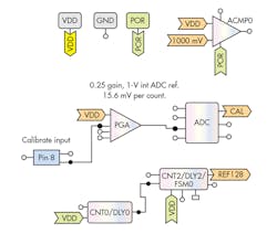
When the actual oscillator frequency is less than 2040 kHz, the STOP value will be somewhat less than 128. How do we push the STOP value using an external trimmer? Enter the analog-to-digital converter (ADC) (Fig. 4, again).
The ADC takes an analog voltage from Pin 8 and generates a digital value labeled CAL that is used by FSM1 as its counter data. When the input voltage at Pin 8 is zero, the CAL value is zero. Increasing the voltage increases the CAL value. In addition, since FSM1 starts counting at the CAL value rather than at zero when it receives a SET signal, it also increases the STOP value.
We now have the following procedure for field calibration when the input signal is known to be at 50.00 Hz. First, the Pin 8 voltage is slowly increased from zero until the STOP value touches 128. At that point, DCMP2, whose IN– pin is fed with the constant reference value of 128 generated by FSM0, outputs a signal on its EQ output that lights up an LED on Pin 17 indicating that the unit is calibrated.
For convenience, the calibration input voltage for Pin 8 could be generated by using the VREF macrocell to output a reference voltage of 1 V on Pin 19 and utilizing a trimmer as shown in Fig. 1. (There is a small subtlety here: After field calibration, the STOP value of 128 no longer will be at the exact center of the count range, which is now less than 255; however, this does not cause serious problems because the FSM1 CAL value is expected to be relatively small.)
DCMP0Now comes the relatively simple part—deciding on the reference values for DCMP0/1. From the calculations, we see that a 0.1% error in mains frequency amounts to an error of 2.5 in the STOP value. We chose selectable sensitivity levels of 0.4% and 2%. A 0.4% error equals 10 RC cycles and 2% error equals 50 RC cycles.
Correspondingly, the lower and upper limits for the DCMPs may be set to 128 ±10 or 128 ±50, depending on the desired sensitivity level. The sensitivity level is selectable using a LOW /HIGH input on Pin 20, which feeds the MTRX SEL inputs of the two DCMPs. The DCMPs select from Register 0-3, into which the corresponding bounds are programmed.
Implementation Notes and Results
For the most part, the design can be tested with emulation. The emulation signal generator has a resolution of about 1%, so it is possible to test the basic correctness of the design with a sensitivity not greater than 1%. It is difficult to test a breadboarded unit with mains input because of the stray hum pickup at the ACMP inputs, which causes spurious readings.
The author tested this design under emulation, where the calibration input to Pin 8 was via emulation, and the waveform input at Pin 12 was from a Tektronix SG502 square-wave generator set to 50 Hz. Time periods were verified using a Tektronix DC503A counter reading the time period at 0.001-ms resolution. The unit under emulation attained calibration at a Pin 8 voltage of about 440 mV, corresponding to a CAL value of about 28. Subsequently, the design worked correctly at both low and high sensitivities.
This is a simple but useful design for a mains frequency monitor. The design can be used for simple alert or data-collection purposes, or be made a part of a more elaborate feedback loop or changeover/shutdown circuitry in an inverter design. In a real implementation, take care to lay out the circuit and provide adequate shielding so that no noise or hum exists at the ACMP input that could cause spurious triggering and affect reliability.
