Key Electroplating Elements For Power Semiconductor Assembly
Fundamental materials properties of the plated layer (such as purity and microstructure) are critical for die attach and wirebond, and the specific plating strategies that can yield these properties. Therefore, we will consider:
•Plated layer qualities that produce high reliability solder die attach interfaces;
• Plated layer qualities that produce high reliability wirebonds after the heat exposure associated with solder die attach (or other assembly operations).
PLATED PAD REQUIREMENTS
For solder related die attach processes, the biggest threat to reliability is from the formation of thick, continuous layers of intermetallic compounds (IMC) under the solder . These layers form from the chemical reaction between the solder and the plated metallization layer on the die attach pad during the die attach process. The type of solder, processing conditions such as time and temperature, as well as the thickness and chemical make-up of the plated pads will play a role in determining IMC layer structure.
Typically, IMC materials are mechanically brittle and have low thermal and electrical conductivity, poor qualities for a die attach pad. A listing of some common IMC materials found in assembly processes is shown in Table 1along with a listing of some key properties. Note from this figure that two very ductile metals, such as Cu and Sn, can react to form a very brittle IMC.
Metallic pads will have a very large CTE relative to semiconductor die. For example, the CTE of Cu is 17 ppm/C and Si is 3.5 ppm/C. This means that during cooling from die attach or subsequent temperature excursions, a CTE mismatch stress will develop between the pad material and the device. If the board material is made of a ceramic, a similar stress will develop between the board material and the pad. For example, Al2O3 has a CTE of about 8 ppm/C.
This CTE stress is the fundamental reason that a thick, continuous brittle IMC layer is a reliability issue. Under stress, a crack can form and easily propagate through this IMC layer, or between two different IMC layers if present at the interface.
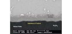
Fig. 1. Failure interface between two IMC layers. SAC solder on Ni/Au plating.
Fig. 1 is a micrograph that shows a solder die attach structure with two different IMC layers that are both continuous and about 1 micron thick: Ni-Cu-Sn and Ni3Sn4. Above the top Ni-Cu-Sn IMC is SAC 305 solder. A failure was seen between the two IMC structures after temperature cycling (the failure interface is sketched in the figure). As a general guideline, IMC layers that are continuous and >1µm thick are potential candidates for interfacial failure.
As a consequence, one key role of the plated layer is to limit the thickness of IMC formation during the die attach process as much as possible for a given set of processing conditions. How this can be accomplished will be discussed in the next section of this article.
Of course, any type of solder die attach process will mean that the plated metallization system is exposed to elevated temperatures during the die attach cycle, which includes the ramp up to die attach, hold at die attach temperature and ramp down cycle. Depending on the type of solder, this can range from 200°C for PbSn eutectic (20°C above the eutectic melting temperature), 235°C for Sn-Ag-Cu (melting temperature 217C), 300°C for AuSn and up to 420°C for Au-Si.
During this temperature cycle, there can be subtle but very significant changes in the chemistry of plated layers, which can have a significant impact on wirebond reliability.
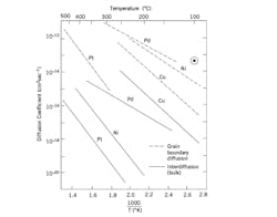
Fig. 2. Bulk and Grain Boundary Diffusion of Various Metals in Au[3] .
Fig. 2 is a very well-known data from “Wirebonding in Microelectronics Materials, Processes, Reliability and Yield” by George Harman .
This data shows the bulk and grain boundary diffusion of various metals in Au as a function of temperature. For most packaging applications, plated Ni or Pd is utilized below the Au bonding surface. Note that the diffusion coefficient for Ni along the Au grain boundaries is 7 to 8 orders of magnitude faster than diffusion of Ni through the Au grains.
Particularly in an atmosphere that is oxidizing for Ni, there is strong chemical driving force for Ni to diffuse to the surface of the Au. Even at concentrations of 2-3%, Ni on the Au surface will have a significant effect on wirebond reliability3.
Consequently, when Ni/Au plated surfaces are exposed to elevated temperatures during die attach, it is critical to limit the Ni diffusion through the Au grain boundaries to the surface of the Au. It is clear from Fig. 2 that the amount of Ni grain boundary diffusion will increase significantly with increasing die attach temperature, making this problem very critical for higher melting temperature, hard solder die attach materials such as AuSn, AuGe and AuSi.
The discussion above illustrates that the wirebonding process is very sensitive to impurities on the surface of the wirebond pad. Another critical wirebond pad property, which is also related to impurities, is hardness.
During thermo-sonic bonding, the harder the pad material, the more difficult to form the atomic intermixing of the wire and pad material that is critical for initial bond formation. For example, for an electroplated Au pad, hardness values below 90 HV are targeted for effective wirebonding. Starting with very soft Au is important since some level of work hardening will occur (even for Au) during thermo-sonic bonding. Controlling impurities such as Ni, Cu and C will be critical for achieving this type of ductility in the plated layer.
In summary, there are a number of critical material’s related functions that must be “built into” the plated layer for assembly processes that entail die attach followed by wirebonding:
• The plated pad metallization must minimize formation of thick, continuous IMC layers during die attach
• The plated wirebond pads surface must remain free of foreign metallic impurities that may diffuse from under-layers during elevated temperature cycles associated with die attach.
• The plated wirebond pad must be highly ductile to maximize as-bonded interfacial area between the wire bond pad and the wire.
Minimizing Thick Continuous IMC Formation During Solder
Thick IMC formation can be effected by plated layer characteristics in two broad areas. The first is by limiting the supply of a material that contributes to IMC formation
during solder reactions. The second is by altering plated layer chemistry so that the rate of IMC formation can be diminished. Examples of each of these situations will be described below.
The most well-known example of limiting the available quantity of a material that aggressively contributes to detrimental IMC formation is limiting Au pad thickness for Sn containing solders such as PbSn, or Ag-Cu-Sn.
Au will readily form AuSn IMC phases such as: AuSn4, AuSn2 and AuSn. These phases, typical of IMC materials, are brittle. When the available Au supply is very limited, and these IMC phases are thin and/or discontinuous, then reliability issues associated with brittle Au intermetallic compounds are not observed. However, for Au layers thicker than approximately 30 micro-inches (depending on the specifics of the process), reliability issues due to AuSn IMC formation become a concern.
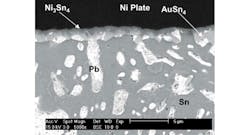
Fig. 3. NiSn and AuSn IMC at PbSn Ball interface with Plated Ni/Au.
Fig. 3 shows two thick, continuous IMC layers at the interface between a Ni/Au plated pad and a PbSn solder ball. The first is Ni3Sn4 and the second is AuSn4. This is an example of a solder interface where potential “Au embrittlement” issues could occur.
Since wirebonding (as will be discussed later) typically favors thicker Au layers, there is a balancing act between robust die attach and robust wirebonding.
The situation where plated layer chemistry can limit the reactive formation of a thick, continuous IMC layer is well illustrated for AuSi die attach.
AuSi has the highest processing temperature of the Au containing hard solder die attach materials. It is processed at 420C or higher. AuSi is used in very high thermal demand applications because of its outstanding thermal conductivity of over 250 W/m-K.
One of the major reliability issues associated with AuSi die attach is formation of a thick, continuous NiSi2 layer under the AuSi. When the AuSi solder melts it will dissolve the adjacent plated Au layer. Consequently, the plated Ni layer will react with the liquid solder, and a nickel silicide layer will form.
Because NiSi2 is a very brittle intermetallic, during die shear stress the nickel silicide layer will crack and the die will easily pop off the pad. This failure is shown in Fig. 4.In this case, the NiSi2 layer is >1µm thick.
Fig. 4. Crack Through NiSi2 layer below AuSi Die Attach.
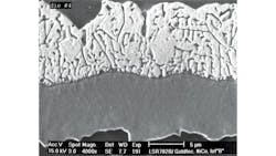
One excellent option for limiting the growth of NiSi2 during AuSi die attach is to co-deposit Co with Ni to produce a Ni80Co20 co-plated layer under the plated Au. Because Co will form a silicide at a much slower rate than Ni, the NiCo/AuSi interface quickly becomes rich in Co silicide. This layer then acts as a barrier to Ni diffusion and thus limits the growth of the Ni silicide layer. Fig. 5 shows a NiSi2 layer that is about 0.24 microns thick after AuSi die attach on plated Au on top of co-deposited Ni with 20% Co.
Fig. 5. Very thin NiSi layer with plated Ni co-deposited with 20% Co.
In this case, die shear measurements result in die fracture, not delamination at the die/pad interface.
REFERENCES
1. Advanced Microelectronics, July/August 2008, Vol 35, No. 4, pg. 22, J. Harris and E. Rubel, “The Role of Intermetallic Compound Formation on Package Reliability”
2. Fields and Low, NIST Metallurgical Division, Research Publication
3. George Harman, Wirebonding in Microelectronics Materials, Processes, Reliability and Yield, McGraw Hill, 1997
