DKN Research Co-Develops Thin Metal-Free Flexible Circuits
July 23, 2013
Comments
Comments
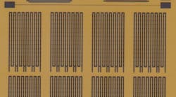
DKN Research, a leading engineering firm specializing in microelectronics and packaging technology, now carries thin metal-free flexible circuits with reliable via holes. The Haverhill Massachusetts based firm developed a series of processing technologies to generate thin graphite traces on both sides of thin polyimide film specifically targeting those scientific and medical applications that require the elimination of metals that have large atomic numbers and weights from electronic devices. It also provides a wider range of design flexibilities for packaging and termination in special electronic circuits. DKN Research continually develops a wide range of packaging technologies for printable & flexible electronics.
Virtually all printed circuit boards use copper foils or the other metals for their conductive material because of its high conductivity and long experience in the electronics industry. Unfortunately, several electronic devices designed for scientific and medical equipment prefer to eliminate metallic elements including copper and silver in the circuit because of its physical nuclear reactions with heavy atoms. Several researchers are now considering conductive polymers as the conductor materials for electronic circuits. However, the conductivities from the organic compounds are still low. There is still a lot of R&D needed so a patterning process can be established to produce practical electronic circuits.
DKN Research partnered with Pyramid Technical Consultants, Inc, a specialty electronic module manufacturer from Lexington Massachusetts, and co-developed many kinds of copper-free flexible circuits combining various technologies such as sputtering, plating, chemical etching and laser ablation & drilling. The team recently announced the success in establishing a new manufacturing process to generate thin graphite traces down to 10 microns thick on both sides of thin polyimide film with small via hole connections down to 80 micron diameters. Special polyimide etching process and laser drilling process were employed to generate tiny holes on thin polyimide films. A new screen-printing process was developed to make uniform conductive layers on the surface and inside the polyimide film holes. A set of screen-printing process and laser abrasion process were furnished to make fine traces down to 100 microns line and space. The conductor resistance of the printed pattern is smaller than 100 ohms/square, that is much lower than traditional carbon paste. The small via holes formed by this new process are very reliable, and remained intact during the heat cycle and flexing endurance tests.
DKN Research and Pyramid Technical Consultants agreed to disclose all the information pertaining to their new technology and share the unique process with other researchers and engineers. This unique circuit manufacturing can work with other circuit processing technologies such as copper etching and screen-printing to enhance the capabilities of any special application. Technical reports are available by requests, and the two engineering teams can support both prototype trials and volume productions.
