Applying Synchronous Rectification in Resonant Half-Bridge Converters
Technology developed for driving synchronous FETs in flyback topologies can be directly applied in LLC topologies. This technology offers significant gains in efficiency for applications with low output voltages, and high output currents.
Related Articles
- Digital Control Provides LLC Performance Enhancements
- LLC Resonant Converters Increase Efficiency in DC-to-DC Applications
- Understanding the Data Sheet Key to Effective Circuit Design
- New Technique for Non-Invasive Testing of Regulator Stability
- Topology Key to Power Density in Isolated DC-DC Converters
- Source Impedance Affects Converter Performance
Resonant half-bridge converters provide a cost-effective and efficient solution for offline power supplies in the range of 200 W to 500 W. This topology is also known as an LLC converter, with the name derived from the fact that the resonant tank comprises two inductors and one capacitor. The transformer's magnetizing inductance accounts for one of the inductors. The other inductor can be either a separate component, or integrated into the power transformer in the form of leakage inductance. This topology benefits from zero voltage switching on the primary switches and as such has been traditionally applied in applications with high input voltages, where switching losses are more dominant. In LLC converters with lower output voltages, losses in the output diodes can be a thermal problem. Replacing them with synchronous rectifiers can reduce losses and increase efficiency, as well as reduce size by eliminating bulky heat sinks.
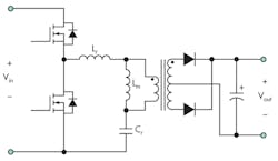
Fig. 1 shows a simplified schematic of an LLC converter. The primary FETs are driven out of phase with each other at a 50% duty cycle. The switching frequency is variable and is controlled to regulate the output voltage. The gain characteristics of the power stage determine the switching frequency at a given input voltage and loading operating point. For proper function, the convert must always operate in the inductive region, to the right of resonance. In high current applications, the secondary of the power transformer is often configured as a current-doubler (Fig. 1). Each secondary winding and diode conducts only half of the current that otherwise would flow in a transformer with a single secondary.
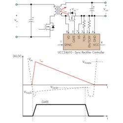
A class of synchronous rectifier controller/driver exists that originally was intended for use in discontinuous flyback converters. These devices essentially control a MOSFET in such a manner that it is on when current begins to flow source-to-drain through the body diode, and off when the current drops below a certain level. Since these devices only allow current to flow in one direction, they mimic the action of a diode with low loss and can be referred to as ideal diode emulators. Fig. 2 shows how this is typically implemented in a flyback converter.
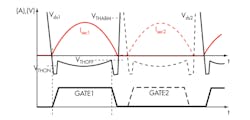
In Fig. 2, the current direction and amplitude is detected by monitoring the voltage on the drain connection of the synchronous rectifier. When the primary FET is turned on, the voltage on the drain of the synchronous rectifier transitions past the VTHARM threshold and arms the driver. When the primary FET is turned off, current begins to flow through the body diode of the synchronous rectifier. The driver detects the negative potential (VTHON) on the drain, and turns on the synchronous FET. As the secondary current decays, so does the voltage on the drain of the Synchronous FET. When this voltage drops below a threshold (VTHOFF),the driver turns off the synchronous FET and waitsto be armed for the next switching cycle. The voltage on the source pin is also sensed through a kelvin connection for a more accurate monitoring of the drain-to-source voltage.
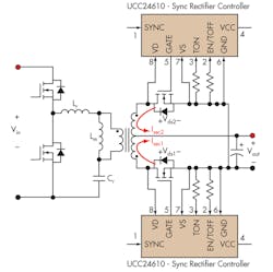
Luckily, it turns out that the secondary voltage and current waveforms in LLC convertersare well-suited for ideal diode emulators. The secondary windings act as a current source, forcing the conduction of the output diodes. As shown in Fig. 3, two drivers and two synchronous rectifiers are required; one driver and one synchronous rectifier for each secondary winding. The driver is armed when the opposite secondary rectifier is conducting. The current waveform's generally sinusoidal shape provides a gradually decaying slope allowing plenty of time for the synchronous rectifier controller to detect the VTHOFFcrossing and turn off the synchronous FET.
The rising edge of the secondary current can pose a potential problem. Because the current begins from zero, the drain to source voltage will be below the turn off threshold at the start of the conduction cycle. Most synchronous rectifier drivers provide a minimum on-time function that masks the turn-off comparator to prevent false triggering due to noise. In LLC applications, it is critical to use a synchronous rectifier driver that provides this function. The minimum on-time should be set long enough to ensure that the drain to source voltage has risen above the turn-off threshold.
As a practical example, consider an application that requires a 12 V, 460 W output to be derived from the output of a PFC pre-regulator. With a 38 A output current, the currents in each of the secondary windings are 19 A (average) and 30 A (rms) per winding. Assuming a forward drop of 0.5 V, Schottky diodes would dissipate around 19 W. This would require significant heat sinking. The advantage offered by synchronous rectification is immediately obvious. With a current doubler configuration, thesynchronous FETs must be rated for at least two times the output voltage plus margin. In this application, 40 V FETs are a good choice. Using three paralleled 3 mΩ FETs limits the dissipation to around 330 mW per FET. There will be some additional loss during the short durations near the zero crossings, when the body diode is conducting. The synchronous rectifiers offera savings of around 17 W compared to using diodes.
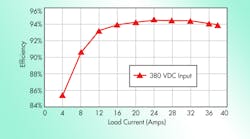
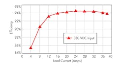
Fig. 4 displays the efficiency measured on a prototype of this 12 V, 460 W design. The synchronous rectifiers provide efficiencies over 94% for much of the load range. By comparison, with Schottky diodes, the efficiency would be around91% at the full 38 A load.
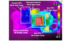
The losses in the synchronous FETs are low enough that surface mount components can be used with some forced air flow, eliminating heat sinks, which reduces the size and simplifies the assembly process. A thermal image of the prototype, Fig. 5, shows that the temperature rise of the synchronous FETs is less than 40 ºC. In fact, the rectifiers are no longer the hottest components on the circuit board.
References
1. PMP 5967 datasheet
