Testing GaN and SiC Devices: FAQs
Why do GaN and SiC devices need unique test equipment? Power semiconductors employing silicon carbide (SiC) and gallium nitride (GaN) have higher power density, smaller size, better high temperature performance, higher frequency response, and lower ON resistance than their silicon counterparts. Plus, these devices have lower leakage than silicon, so there is a need for sourcing higher test voltages, as well as appropriate low current measurement sensitivity. For example, SiC leakages are more than two orders of magnitude lower than similarly rated silicon devices, so they require current measurements in the single microamps range.
Related Articles
- Characterizing High Power Semiconductors Requires New Technologies
- Test Equipment Must Keep Pace with New High Power Semiconductor Developments
- EMC Poses Challenge for Automotive Electronics
- AC Power Testing Presents Many Challenges and Concerns
- Test Saturation Voltage to Achieve High Efficiency #1
- Test Saturation Voltage to Achieve High Efficiency #2
Dynamic testing of devices switching kilowatts in microseconds requires advanced driver circuits and very well designed interconnect and layout of tester electronics as well as device-under-test sockets and contactors. Safe and reliable results requires tight design for creepage and clearances. Also, very fast, high power transition times requires attention to ground noise and EMI.
What are the voltage and current requirements to test GaN and SiC devices? This requires the handling of breakdown voltages up to 3000 V or even higher, more than 100 A, and junction capacitances for dc biases up to 3000 V. The tester must be able to withstand high SiC and GaN voltages and fast switching speeds. For best results, it is crucial to test these devices at their specified voltage, current and power rating.
What test equipment is available for use with GaN and SiC transistors? Keithley Instruments has introduced the Parametric Curve Trace configurations , specifically designed for high voltage and current characterization of high power semiconductors. To meet the requirements of the new generation of high power semiconductors, Agilent Technologies Inc. has enhanced its B1505A Power Device Analyzer/Curve Tracer to significantly increase its voltage and current range, allowing it to test GaN and SiC transistors.
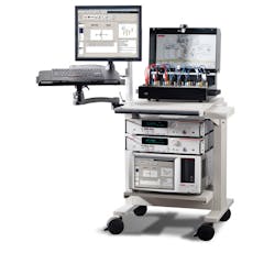
What are the characteristics of Keithley’s Parametric Curve Trace configurations? These flexible configurations will support voltage from µV to 3 KV, and currents from 1 fA to 100 A. These systems are engineered to provide the highest level of measurement performance, while maintaining a safe working environment (Fig. 1). The modular design allows any configuration or power level to be upgraded in the field at any time. The Windows™ user interface supports both interactive trace mode for quick device diagnostics and high precision parametric mode for detailed parameter extraction. One advantage of this independently modular approach is that an appropriate test system can be configured for any application from a simple curve trace tool to data sheet generation to a sophisticated reliability and production test tool.
Other features of the B1505A include:
• All-in-one solution for power device characterization up to 1500 A & 10 kV
• Medium current measurement with high voltage bias (e.g. 500 mA at 1200 V)
• μΩ on-resistance measurement capability
• Accurate, sub-picoamp level, current measurement at high voltage bias
• Capacitance measurement at up to +/- 3 kV DC bias
• 10 μs high power pulse measurement
• Temperature measurement capability
• High voltage/high current fast switch option for GaN current collapse effect characterization
• Automatically switch between high-voltage and high-current measurements without recabling
• Standard test fixtures with safety interlock for packaged power device testing
• Tested and supported high power 200 A on-wafer testing
• MS Windows-based EasyEXPERT software simplifies data management and data analysis
• 10 module slots
• Support for high power devices with up to 6 connection pins
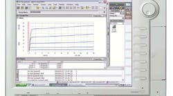
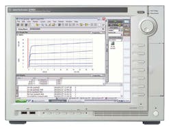
Can you use a curve tracer to check GaN and SiC performance? A curve tracer, such as the B1505A (see Fig 2.), produces I-V (current-voltage) curves that provide a good assessment of device behavior. Therefore, a curve tracer is the ideal instrument to determine the characteristics of these high power, discrete semiconductors. Characterization of SiC and GaN devices requires an appropriate curve tracer with high breakdown voltage measurement capability as well as the ability to measure leakage currents at high voltage biases.
A GaN and SiC curve tracer needs a switch to automatically change the measurement resource between high voltage and high current. Otherwise, the operator must change measurement equipment connections to the device-under-test manually, which can cause trouble.
For best reliability results, I-V characteristics near the safe operating area (SOA) is an important measurement for GaN and SiC devices. When a high voltage is applied to a device, its impedance can change rapidly and apply medium to high current through the device. Using a narrow test pulse (less than 50 µs) prevents device self-heating that could impact accurate characterization. When originally introduced, curve tracers were analog instruments that employed a CRT (cathode ray tube) display. Today, curve tracers have become digitized and use flat panel LCDs to present data. Digital techniques now provide the ability to store measurement data and retrieve it.
Why isn’t older test equipment adequate for GaN and SiC? Leakage current and breakdown voltage determine basic GaN and SiC behavior. Older test equipment, typically limited to the µA level, lacks sufficient resolution and accuracy for leakage characterization. And, if the breakdown voltage is more than 3 kV, older instruments can’t even measure it. Companies have had to design and build a custom test system to measure ultra-high voltage. However, these may have safety and traceability issues.
Can older test equipment measure GaN and SiC on-resistance accurately? GaN and SiC on-resistance is now as low as a few milliohms and continues to decrease, which causes measurement accuracy problems. Accurate measurement of on-resistance requires precise constant current applied to the device using an accurate voltmeter with a full Kelvin connection. Older generation curve tracers don’t have current source capability, which makes it difficult to accurately perform characterization.
A current source mode can aid in accurately measuring GaN and SiC on-resistance. This requires a continuous monitoring and adjustments for the internal feedback circuit used by the current source. This way, set current flows regardless of contact resistance variations and you can measure on-resistance very accurately. In contrast, a voltage source mode for the on-resistance test involves immeasurable contact resistance that causes a voltage drop and degrades the measurement. Pulsed current testing can help control the effects of device self-heating.
Can a test instrument make on-wafer measurements? On-wafer measurements require extension cables to connect the test equipment and prober. In this case, the drive voltage has to be high enough to overcome the IR voltage drop in the extension cable. The GaN or SiC drain or collector supply voltage must have enough margin even when IR voltage drop is high due to high current. To ensure sufficient drive supply voltage requires a special extension cable with low residual resistance. High voltage testing at the wafer level requires a properly designed safety system to prevent the user from exposure to the high voltage. Interlock mechanisms between the prober and the instruments must be used to protect the user.
How important is the test fixture? A proper test fixture solution is extremely important, both to insure safety (due to the high voltages and currents used) and to support the wide variety of power device package types. A previous limitation of curve tracers was that some power devices could not be evaluated due to their size, or it was necessary to jury-rig an adapter in order to test the device. Therefore, you need a test fixture that can accept a wide variety of devices, regardless of their size or shape so the test fixture adapter must be customizable. In addition, the test fixture should have a built-in interlock mechanism to ensure that high voltages and currents do not endanger the device-under-test or the test operator.
One complication is that the existing GaN and SiC semiconductors require unique test fixtures because they may be housed in different packages. Plus, some of the GaN devices are enhanced mode and others are depletion mode with integrated driver circuits. Existing SiC devices now use industry-standard packages, but as their portfolio grows, newer packages will certainly have to be optimized for high-speed, high-power switching.
What are the safety concerns for testing GaN and SiC devices? Safety is a concern when configuring any high voltage test system. Typically, the test systems require safety interlocks, double grounds, and other safety features to protect operators and sensitive system instrumentation. In Europe it requires test and measurement equipment to demonstrate safety by complying with EN61010-1. Internationally it is IEC61010-1 and in the USA it is UL61010-1.


