Electromagnetic Compatibility Part 2: Considerations When Working With Switching Power Supplies
As highlighted towards the end of Part 1 there are two major classes of EMI, conducted and radiated. Conducted EMI can be further subdivided into differential and common mode noise. Here we look at the mitigation techniques for each with additional considerations for switching power supplies and system level EMI mitigation methods.
Related Articles
- Layout Power Supply Boards to Minimize EMI: Part 1
- Layout Power Supply Boards to Minimize EMI: Part 2
- Layout Power Supply Boards to Minimize EMI - Part 3: EMI Basics
- Conforming with Worldwide Safety and EMC/EMI Standards
- Understanding EMI Noise In Power-System Design
- Eliminate the Guesswork in Controlling EMI
Conducted EMI
To effectively mitigate conducted emissions, it is imperative to address the differential mode noise and common mode noise separately - see coupling section in part 1.
Differential mode noise can usually be suppressed by connecting bypass capacitors directly between the power and return lines of the switching power supply.
It’s worth noting, however, the power lines that require filtering may be those located at the input or the output of the switching power supply and the bypass capacitors on these lines need to be physically located adjacent to the terminals of the noise generating source to be most effective.
Furthermore, the actual location of the bypass capacitor is critical for efficient attenuation of differential mode currents at high frequencies.
Attenuation of differential mode currents at lower frequencies around the fundamental switching frequency of the noise generating source may dictate that a much higher value of bypass capacitance is required, meaning a ceramic style capacitor would not be suitable. Ceramic capacitors up to 22 μF are only suitable filtering across the lower voltage outputs of switching power supplies but not for those supplies where 100 V surges can be experienced. Instead, electrolytic capacitors, which have a high capacitance and voltage rating, should be employed.
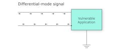
Indeed, to suitably attenuate differential mode current (Fig. 1) both at the lower fundamental switching frequency as well as at the higher harmonic frequencies, differential mode input filters usually consist of a combination of electrolytic and ceramic capacitors.
Further suppression of differential mode currents can be achieved by adding an inductor in series with the main power feed to form a single stage L-C differential mode low pass filter with the bypass capacitor.
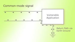
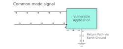
Conversely, common mode conducted currents are effectively suppressed by connecting bypass capacitors between each power line of the switching power supply and ground. These power lines may be at the input and/or output of the switching power supply.
Further suppression of common mode currents (Fig. 2) can be achieved by adding a pair of coupled choke inductors in series with each main power feed. The high impedance of the coupled choke inductors forces common mode currents through the bypass capacitors.
Radiated EMI
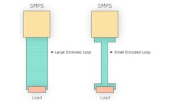
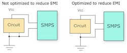
Radiated EMI can be suppressed by reducing RF impedance and reducing the antenna loop area. This is achieved by minimizing the enclosed loop area formed by the power line and its return path (Fig. 3).
The inductance of a printed circuit board track can be minimized by making it as wide as possible and routing it parallel to its return path. Similarly, because the impedance of a wire loop is proportional to its area, reducing the area between the power line and its return path will further reduce its impedance. Within printed circuit boards, this area can be best reduced by placing the power line and return path one above the other on adjacent printed circuit board layers. Reducing the loop area between a power line and its return path not only reduces the RF impedance, but it also limits the effectiveness of the antenna because the smaller loop area produces a reduced electromagnetic field.
Furthermore, a ground plane located on the outer surfaces of the printed circuit board significantly suppresses radiated EMI, particularly if located directly below the noise-generating source.
And to further reduce radiated noise, metal shielding can be utilized, placing the noise-generating source within a grounded conductive housing, and interfacing to the clean outside environment is via in-line filters. Common mode bypass capacitors would also need to be returned to ground on the conductive housing.
EMI Mitigation In Switching Power Supplies
Reliable wiring connections should be implemented to and from the supply. Wiring must be of suitable size and be kept as short as possible, with wiring loops minimized. Avoid running input or output wirings near power devices to prevent noise pick up.
Grounding connections should be properly secured with earth ground wires kept as short as possible. For circuit or system operations that induce current transients it vital to supply the pulsed current locally via decoupling capacitors, rather than letting the pulsed current propagate up stream to the supply. These capacitors should include high frequency ceramic caps and bulk capacitors.
Additionally, if the operation allows, slow down the clock, or the rising/falling edges. And where this is not possible, circuits with higher clock rates/fast switching times should be located close to the power line input to reduce power transients. It is recommended that both analog and digital circuits should be physically isolated on both power supply and signal lines.
Ground loops should be eliminated; especially in complex systems. This can be achieved using a single point ground or a ground plane. An example is highlighted in Fig. 4.
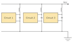
Multiple circuit systems should run separate supply lines and/or place inductance in the supply lines to decouple the circuits. This can be seen in Fig. 5.
Ferrite beads can be placed on the dc supply lines to ac isolate the system and the supply. This can be effective in preventing power switching harmonics disrupting the system’s operation, and prevents system generated noise from reaching the power supply.
On the input side, if the built-in EMI filter is insufficient for a specific application, additional EMI filtering can be applied before the power supply. A bead can also be placed on the earth ground wire between the ac inlet and the supply.
Dc-dc converters have specific considerations that must be addressed and although many of the mitigation techniques highlighted above are applicable to the implementation of both ac-dc power supplies and dc-dc converters within a system, there are additional steps that should be taken for dc-dc converters.
A pulsed input current is demanded for the switching action in most dc-dc converters and this is best supplied by local capacitors close to the switching devices. As many switching dc-dc converters are compact in size, they generally do not contain sufficient capacitance, meaning additional capacitance should be placed at the input to reduce differential mode noise. For even better filtering performance, a PI filter can be employed.
The additional capacitors are used to reduce common mode noise.
System-Level EMI Mitigation Techniques
Although most switching supplies are designed to meet applicable EMI standards as stand-alone modules, the system itself needs be designed to generate a minimum EMI profile to meet regulatory standards. Specific areas in the system design that are candidates for EMI mitigation practices include the signal lines, printed circuit boards (PCB), and solid state components.
Signal line considerations include the use of low pass filters on signal lines to reduce allowable bandwidth to the minimum level that still allows a signal to pass un-attenuated. Feed and return loops should be kept close on wide bandwidth signal lines to minimize radiated emissions. Additionally, signal lines carrying RF or near-RF signals should be properly terminated to reduce reflection at the termination. Ringing and overshoot on these lines can also be minimized as a result of using the appropriate termination.
PCB high impedance runs that contribute to EMI can be mitigated by using wide PCB metal stripes to decrease the impedance of power lines. Where possible, signal tracks should be designed with consideration for their propagation delay vs. signal rise/fall time and include a ground and a power plane. Slit apertures in PCB layout should be strictly avoided, particularly in ground planes or near current paths to reduce unwanted antenna effects. Board metal stripes should be kept as short as is practical, and metal stubs, which can cause reflection and harmonics, should be avoided.
Also, avoid overlapping power planes to reduce system noise and power coupling. Reduce or eliminate sharp bends in metal stripes (also known as beveling or track mitering) to reduce field concentration and run conducting stripes orthogonally between adjacent layers to reduce crosstalk. Floating conductor areas can act as a source of radiated emissions, so their use should be avoided except for overriding thermal considerations. Additionally, solid state components on the PCB should be decoupled close to chip supply lines to reduce component noise and power line transients.
Summary
Switching power supplies generate EMI because of their inherent design. Domestic and international regulatory bodies regulate these emissions through promulgation of rules and standards such as the FCC Part 15 rules and the CISPR 22 standard.
An understanding of EMI fundamentals and best practices to mitigate the different types of EMI when implementing a power supply is crucial in design. However, it is also important to understand that a power supply is just one part of an electronic system with multiple EMI sources, so evaluating the power supply’s EMI performance within a system is vitally important.
For additional power supply information go to www.cui.com.
Visit Part 1: Definitions, Standards, International Regulations and Compliance
