Power Electronics 2014 Forecast Part 1: Power Supplies
The rapid pace of technology advances will be readily evident in the power supply sector this year, according to several industry experts interviewed by Power Electronics. Their thoughts follow.
From Mark Adams, Senior Vice President, CUI Inc.
Three things in life are certain, death, taxes and incremental improvements in technology. But, for the power market, 2014 will break this rule as technological and environmental forces push power from being an afterthought to playing a starring role in next-generation systems.
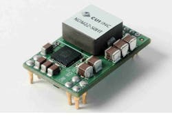
2013 saw emerging power technologies begin to move to the mainstream. Digital power supplies became, if not mainstream then, a non-niche product. The early adopters (mostly telecom and datacom OEMs) were joined by smaller companies from multiple industries; driven by a need to address the power challenges of the latest generation ICs, and a move by digital power vendors towards simpler methods of implementation. Fig. 1 shows a 50 A power supply that employs auto compensation.
2014, in my view, is going to see two key issues come to a head and drive further growth and innovation in advanced power technologies:
1) Moore’s Law
2) Limitations in existing power topologies
Moore’s Law & Digital Power
Ever-shrinking chip architectures are now reaching a point where their sensitivity and complexity require tighter tolerances in the power specifications, and where variability in manufacturing is decreasing yields and increasing cost.
One way to increase yields is to require a dynamically adjustable core voltage, which can be achieved by applying digital power at the socket level.
The importance of dynamic control is also reflected in PMBus V1.3 and its adaptive voltage scaling bus (AVSBus), which creates a closed-loop, real-time feedback voltage control system to handle process and temperature variations between devices, continuously updating the voltage requested from the power supply.
We’ll see the dynamic core voltage become a requirement for an increasing number of ICs in the coming year, moving digital power from recommended to required in many applications.
Topologies
As board and system level power densities continue to increase in next generation networking equipment, we’re starting to hit the limits of the existing power topologies.
Breakthroughs are being made, however, and initial tests from our new Solus® Power Topology suggests big gains can be had.
Our approach has been to combine a SEPIC with a conventional buck topology, forming a SEPIC-fed buck converter. Lower voltage and current stresses in the topology, coupled with an inherent gate charge extraction process, reduces switching turn-on losses by 75% and switching turn-off losses by 99% on the control FET.
And distributing the energy delivery among multiple paths reduces circuit conduction losses by nearly 50% and further improves efficiency. This allows the topology to provide 40% more output current without taking up more space.
In short, I believe 2014 is set to be a key year for the power market. Macro factors such as the growth in cloud-based computing and a global focus on reducing energy consumption is creating a fresh perspective on the value of power electronics within the system. We’ll see new topologies that offer significant performance gains, and new market drivers that push digital power to a must have technology.
From Patrick Le Fèvre, Ericsson Power Modules
Ever since the introduction by Ericsson in 2008 of the first fully digitally controlled Point-of-Load (POL) converter and Advanced Bus Converter (ABC), digital power technology has helped make complex power systems significantly simpler. The technology has seen exponential growth in the market through its adoption in a significant number of demanding applications in the Information and Communication Technology (ICT) sector. It has now crossed the chasm of uncertainty that previously existed in the industry and the number of applications employing digital power management and control will accelerate in 2014.
Beginning with the original digital POL, a number of technical innovations have now been implemented, including adaptive loop compensation. This should become a de-facto feature for digital POLs in 2014, while also delivering the ability to systems architects via software such as Ericsson Power Designer to access loop-compensation parameters in the customization of power systems for specific load conditions, transient response and stability.
Another evolution in digital POL technology that is expected to develop in 2014 is the ability for processors, FPGAs and ASICs to communicate with the POL and draw power at precise voltages required by microprocessor cores. This will improve performance, reduce power losses and potentially also improve yield for silicon manufacturers, enabling them to retain silicon that is right at the edge of the optimized voltage distribution. Several joint research projects between silicon and board-power-supply manufacturers are showing much promise and the evolution of the PMBus to the so-called PMBus+ (v1.3), enabling energy management at the system level, is certainly going in the right direction.
The use of isolated dc/dc converters and especially Intermediate Bus Converters and Advanced Bus Converters will also become important next year and beyond to bring energy savings in global data network facilities. According to the latest Ericsson Mobility Report, the number of mobile subscriptions globally is estimated to increase from 6.6 billion in 2013 to 9.3 billion in 2019; and clearly this will come with a corresponding increase in the volume of data transferred through networks. In addition, this rise in mobile combined with fixed-line data will require more computing and storage capacity. This will mean that systems designers will need to increase the number of processors per board, resulting in an increase in power demand to more than 1kW per board with a projection that this will reach up to 3kW by the beginning of 2015.
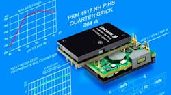
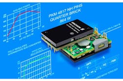
It seems likely that ICT optical routers will require 2 kW per board in 2014, placing challenges on systems designers and board-power manufacturers to not only develop energy-efficient solutions but also consider new packaging that is better suited to this level of power delivered by the latest conventional quarter-brick power modules. If products such as the Ericsson PKM4817NH-PIHS can deliver up to 864W in a quarter-brick format (Fig. 2), systems architects are starting to question if the traditional way of putting quarter-bricks in parallel is really the way forward.
Considering that dc/dc board-mounted power supplies’ (BMPS) are connected via conventional pins that each carry more than 100A to boards that may have in excess of 30 layers, the soldering of these modules becomes highly critical; and in the case of module replacement, rework is extremely complicated. In addition, kilowatt boards will require new cooling methods such as heat pipes connected to cold-plates, so designers of dc/dc BMPS will need to rethink packaging to improve both the assembling process and cooling. Much research is on-going exploring new solutions, which shows a square module with screws to be fixed on high-current press-fit power taps.
Other research projects into kilowatt-power boards, such as Fragmented Power Distribution, are combining highly efficient analog powertrains with digital power management. This technology is still at an early stage of research, but it is one of the most promising technologies to make it possible to optimize energy distribution and utilization when the power per board reaches 3kW.
2013 has been a very exciting year for power designers and systems architects, but 2014 will be even more exciting. And that is even without talking about new materials such as gallium nitride or silicon carbide, which should move from research labs to being deployed in a range of kilowatt-powered board applications.
From Gary Gill, Director, VI Chip Product Line, Vicor
With every generation, electronic products shrink while functionality expands and performance improves. Despite efforts to hold the line on product power dissipation, pressure to increase power density in energy management subsystems continues unabated. This trend, unfortunately, exacerbates the challenging thermal design task facing product development teams.
Most components, and certainly most power dissipating components, within power conversion modules mount to the top side of the converter module’s PCB. For simplicity, most product designs cool power modules and power ICs through their top surfaces. There are, however, multiple heat sinking paths available. As product requirements drive power densities higher, thermal design approaches more sophisticated than simple topside cooling are emerging. In 2014 we’ll see accelerating adoption of these design approaches.
New power packaging technologies and materials allow OEM designers to depart from topside dominant cooling. Power-train designs that arrange dissipative components symmetrically on both sides of a module’s PCB coupled with highly thermally conductive packaging materials allow substantial cooling through the package’s top and bottom surfaces. Additionally, this arrangement can shrink the module’s layout, increasing power density while increasing efficiency by reducing I2R losses in the interconnecting copper traces.
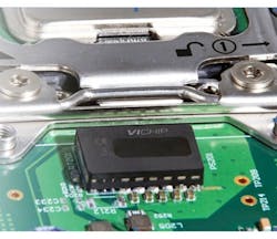
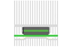
Vicor’s Converter housed in Package (ChiP) is optimized for two-sided cooling, presenting similar thermal resistances through top and bottom surfaces. ChiP packaging supports power management functions such as AC-DC conversion with power factor correction (PFC); isolated bus conversion; dc/dc conversion; buck, boost, and buck-boost regulation; and PoL current multiplication (Fig. 3).
For power components that are thermally limited, two-sided cooling can extend the device’s derating curve tens of degrees toward higher ambient operating temperatures. Conversely, for applications that can maintain modest ambient temperatures, two-sided cooling allows designers to exploit power components for extremely high power densities. The packaging technology is scalable with sizes ranging from 0623 (6 x 23 mm) to 6123 (61 x 23 mm) and expanding, output currents to 180 A, voltages to 430 V and rising, and power delivery to 1.5 kW and rising. With these characteristics, ChiP-based power components realize power densities up to 3 kW/in3 and area densities up to 850 W/in2 with efficiencies as high as 98%.
Power components exploiting ChiP technology can provide exceptional thermal performance in two-sided cooling applications (Fig. 4). The thermal-management cell, depicted schematically in the figure, targets an RθJ-A (junction-to-ambient thermal resistance) less than 0.66 °C/W, allowing for dissipation greater than 60 W at 70 °C ambient. The thermal-management cell concept supports power densities in excess of 200 W/in3 and outputs to 1.8 kW/cell with 400 VDC inputs under the same ambient conditions. The cell uses a single 40 x 40 mm fan to cool both top and bottom heat sinks and is inherently scalable for larger outputs.
Leveraging advanced magnetic structures integrated within high density interconnect (HDI) substrates with power semiconductors and control ASICs, ChiP-based power components can provide unrivaled power density and thermal management agility, and facilitate a modular power system design methodology that minimizes overall design complexity.
