Protecting Boosted Loads and Their Sources
Output short-circuit faults, overload conditions, other fault conditions, and high capacitance loads at startup can seriously strain or bring down an input supply, as well as damage the load. The loads themselves can be demanding, even requiring higher voltages than provided by the primary input supply. These conditions and demands cause input supplies to be overdesigned or overburdened, especially when boosted loads are required. The problem with the common choice of a step-up (boost) converter for the higher voltage load is that it does not naturally provide system protection to downstream circuitry. This is due to the inherent pass path from input to output, which exacerbates the strain on the primary supply and decreases system reliability, especially during fault or overload conditions.
Low-voltage battery-powered systems are one example where loads can require a higher voltage than what the main supply provides. Industrial systems with fixed bus supplies provided over long cables and communications systems with high-efficiency power amplifiers often need a boosted voltage from a wide-input-voltage-range DC/DC regulator.
Register or Sign in below to download the full article in .PDF format, including high resolution graphics and schematics when applicable.
-----------------------------------------------------------------------------------------
This file type includes high resolution graphics and schematics when applicable.
A boosted supply has some system advantages. In systems with large wiring harnesses, a high voltage reduces the wire gauge required to deliver the total power. The automotive industry has been analyzing the problem of expensive and heavy cabling by looking into 48-V batteries. Systems with high-power amplifiers such as RF transmitters find increased efficiency and more output power density from new transistors operating from higher supplier voltages. Some mission-critical systems require reserve power via capacitive energy storage, which requires less capacitance at a higher voltage (E = 1/2*C*V2). A boosted hold-up circuit can result in a smaller solution size.
Failing to consider a boost converter’s natural limitations results in decreased system reliability and added cost, leading to overdesign in other parts of the system. A boost has a natural pass path from input to output (Fig. 1). Even when the converter is shut down, current can flow to the output through the boost diode or body diode of the synchronous power FET.
If the load is heavily capacitive, the main source or battery must bear the burden of the inrush current, since the boost converter does not provide any load isolation.
Without the presence of a separate current-throttling mechanism, this results in an overspecified primary supply. In systems requiring battery backup such as an alarm system, uncontrolled current draw can affect battery reliability or require a larger battery. Even expected heavy-load conditions can cause enough droop on a limited supply (like a battery) to brown out circuitry on the other system rails and produce an unintended system restart. Modular systems powered from a shared supply bus are also at risk during startup. Without inrush limiting or coordinated power-up sequencing, the supply bus may limit the number of allowable modules based on the maximum supply-current capability.
Faulty loads, such as a motor stalling when overloaded, draw heavy currents. A solenoid, as used in injectors, is another example of a load known to fail short. Pluggable modules with motors may need a boosted rail (provided by the main system) to save space and cost in the removable assembly, but may also overdraw the main supply during a hot-plug event. An unprotected boost converter is not equipped to mitigate these risks; it just passes the burden upstream to the supply. Designers often address the problem by overdesigning and overspending on the primary supply, but some simple limiting and protection techniques can save system cost and increase reliability even if a boosted load proves faulty.
Protection Methods
The simplest current-limiting scheme is to employ a negative temperature coefficient (NTC) thermistor (Fig. 2). With high impedance when cold, the NTC initially limits the inrush current during startup. As it self-heats from its own power dissipation, the impedance reduces, allowing more current to flow. The benefits of this method include simplicity and a low-cost protection solution.
The disadvantages come during implementation under harsh conditions. A widely varying temperature environment like a car engine compartment could see high ambient temperatures that reduce the NTC’s initial impedance and allow more inrush current than desired if not carefully managed for the full ambient operating conditions. If a restart condition occurs, the NTC device temperature may not cool before the next power-up. The output capacitance may be fully discharged, but the inrush limiting from the NTC is minimal due to slower thermal dissipation. Additionally, if a load fails short, the NTC will not be able to limit the supply current any more than the nominal operating condition for which it was selected. Ultimately, the NTC approach can be effective for single-function protection but is limited as a passive component.
Turning to an active limiting device like a MOSFET requires a control circuit like an inrush limiting controller, also known as a hot-swap controller or electronic fuse. While this is an additional integrated circuit (IC) in front of the boost controller, many such controllers (Fig. 3) feature programmable inrush limiting with a current and voltage loop controls the inrush rate while ensuring that the MOSFET remains in the safe operating area (SOA). The SOA monitoring maintains long-term reliability for the critical protection device. Additionally, the inrush controller may have two current thresholds: one for standard inrush limiting and a second to implement a circuit-breaker function for severe overcurrent conditions. The clear advantage of this implementation is the advanced protection features that you can achieve; however, the cost and complexity of this solution is generally greater in comparison to the passive approach.
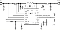
A third protection option is a boost controller with integrated inrush limiting control. This method still requires an additional MOSFET as the protection device, since the boost’s high-side element (a freewheeling diode or synchronous MOSFET) cannot be reversed. However, the integration of the boost and protection control into one IC, as shown in Fig. 4, helps reduce solution complexity and size in comparison with the hot-swap controller method, while providing many additional protection features.
Select a MOSFET for Worst-case Conditions
Any limiting method requires thoughtful design to ensure a robust solution, particularly giving consideration to the power-dissipating device. When using a MOSFET, make sure to account for the safe operating area of the device. Set current is but one parameter to consider. When choosing the MOSFET, factor in the peak stand-off voltage (drain/source voltage), and the length of time it will be under the combination of extreme conditions.
Depending on the system design requirements, the below equations will aid in selecting a MOSFET with a sufficient avalanche energy rating by calculating the peak energy seen by the protection device in these conditions: inrush, output short circuit and abrupt circuit breaker.
Charging energy for inrush considerations is:
Where:
EINRUSH = Output capacitor charging energy in J.
COUT = Maximum output capacitance in F
VINMAX = Maximum input supply voltage in V
While the worst-case output capacitor charging current initially looks like a short circuit, a true short-circuit fault condition can be more demanding on the MOSFET. The short-circuit energy that the MOSFET must survive is dependent on:
Where:
ESHORT = Short circuit protection energy in J
IINRUSH(TH) = Inrush current limit threshold in A.
tDELAY = Delay time in sec
The selected protection controller may have a fail-safe circuit-breaker current threshold, triggering immediate input disconnection. The energy calculation for the circuit breaker is similar to the short-circuit condition but with a different current threshold set by the protection controller, if available. The worst-case energy that the MOSFET could see is calculated for the controller’s response or delay time.
Where:
ECIRCUIT_BREAKER = Circuit-breaker protection energy in J
ICIRCUIT_BREAKER(TH) = circuit-breaker threshold current in A
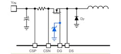
Keep in mind that using a MOSFET for protection allows a quick response to inrush or fault conditions, and you should implement appropriate voltage snubbing on the output side of the MOSFET to ensure that the device intended for protection does not cause problems for the downstream circuitry. With a boost, the first in-line component seen after the protection device is the primary inductor. A freewheeling diode can manage any voltage ringing between the protection MOSFET and the inductor. It only conducts when the protection switch turns off quickly, especially in the circuit-breaker scenario to the left of the inductor (Fig. 5).
Additional Protection Features
Another feature you may want to consider when selecting a protection controller is a retry timer, also known as hiccup mode. If the equipment experiences an intermittent overcurrent fault, it may be to the system’s benefit to automatically retry without requiring a full system restart. Hiccup mode allows the protection controller to open the MOSFET and wait a certain amount of time for the fault to be resolved, then retry by initiating the inrush control sequence. A controller may retry indefinitely, if the fault persists, or it may latch off after a certain number of retries.
A secondary advantage to using a MOSFET as a protection device is the implementation of a crude input overvoltage protection circuit (/). By connecting an appropriately chosen zener diode from the gate of the MOSFET, the gate-to-source voltage of the FET is clamped by the diode, which causes the MOSFET to pull back into ohmic operation as the source voltage increases. The breakdown voltage of the diode sets the effective output-voltage clamp value. The MOSFET acts as a linear regulator while in the ohmic region, but note that the maximum allowable clamping time will be limited by the property of the MOSFET.
References
- Download these datasheets: LM5121, LM5069
- Designing fault protection circuits using wide VIN LM5121, Application Report (SNVA726), Texas Instruments, January 2015
- LM5060 High-side protection controller with low quiescent current (SNVS628), Texas Instruments, April 2013
- CSD19536KCS 100 V N-Channel NexFET™ Power MOSFET (SLPS485), Texas Instruments, October 2014
- Robust hot-swap design, Application Report (SLVA673), Texas Instruments, November 2014
- GaN devices for highly efficient power amplifiers, T. Kikkawa et al. Fujitsu Scientific & Technical Journal. Vol. 48, No. 1, January 2012
- Upgrading the on-board power-net from 12V will pave way for 48V power net, Frost & Sullivan, June 2012


