Power System Insight Using Mathematical Modeling
Using mathematical software to fully model Synchronous Buck Converter (SBC) performance in symbolic form is a tool that is available right now. This allows you to encapsulate the entire system in a set of equations. Once done, by manipulating these equations the engineer can gain an in-depth understanding of the system extents and limitations.
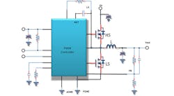
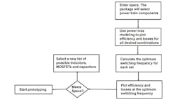
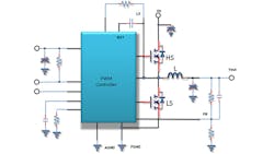
Any mathematical model must be fully reviewed and verified against thorough lab testing and comparing the lab results to the mathematical model predictions. The mathematical package we used for this paper has proven its versatility and accuracy as it was used in the design of several evaluation boards and multiple customer designs. Figure 1a shows a typical flow chart of the design and optimization cycle for the circuit in Fig. 1b.
To elaborate, the loss mechanisms and the equations that govern SBC in modern converters are very well understood.
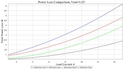
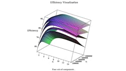
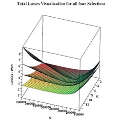
Both Figs. 2 and 3 clearly show that selection 4 is best and may be optimized further by selecting the best switching frequency.
Optimization
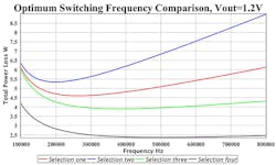
Use of a mathematical model, once complete and verified by lab results, is so simple and literally takes less than an hour to optimize the power train components for a given implementation of any SBC. Once the best four sets of components have been chosen, the next step is to find the optimum switching frequency that will result in the lowest losses and highest efficiency.
Here, we will only consider the losses in synchronous buck converters for investigations and lab verifications. These losses are due to:
- MOSFET conduction and switching
- Inductor core and RDC
- Gate driver
- Output capacitor ESR
- Parasitic losses due to source inductance[7]
- Bonding wires losses
Components Selection
Selection of the best power-train components like MOSFETs and inductor for a given application is the most critical step in the design of a synchronous buck converter. With literally thousands of potential candidates on the market with different prices and parameters, a short cut to selection must be found to enable the engineer to continue to generate quality products at the right price and, very importantly, on time.
The first step is to compile the best table of potentially suitable power-train components based on losses. This is done using the loss equations in a simple loop to sift through the internal database of components and find the top 10 candidates each of high-side and low-side MOSFETs and inductors. Since there are factors that govern the design such as price, size, and availability, the engineer will have to narrow this selection down to four or five sets. Entering the component sets’ parameters into the math model, power loss and efficiency predictions can be generated in seconds once the software is initialized.
Visualization
One of the greatest advantages of this math model is the ability to visualize the extent of the design performance over the key parameters. Figure 4 is a 3D model of efficiency as a function of the switching frequency. One conclusion from this figure is that the top selection has both high efficiency and lower dependency on the switching frequency while the bottom selection is not suitable for any real life application. Figure 5 is a 3D graph showing the losses as a function of frequency and current. A very clear view of the performance of the system is emerging with deep understanding of all the losses under different conditions of current and switching frequency.
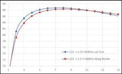
The choice of the switching is crucial in determining the PCB area, component size and overall efficiency of the power supply. This frequency can either be chosen experimentally by building a prototype board where different MOSFETs and inductors of different parameters. Figure 6 shows the efficiency of the selected optimum set operating at 500 KHz clearly showing the accuracy of the mathematical model. In Figs. 5 and 7, we examine the total losses of the four finalist sets that have a single controller but different MOSFETs and inductors.
Loss Equations
Where:
MHSLosses = Control MOSFET losses
ILrms = RMS value of the inductor current
RdsonMHS = Control MOSFET On resistance
Ds = duty cycle
IL = Inductor current
IRIPPLE = Ripple current
VIN = Input voltage
fS = Switching frequency
tR = Rise time of the switch node voltage
tF = Fall time of the switch node voltage
QRR = Reverse recovery charge of the synchronous rectifier
PHSCOSS = capacitive losses of the Drain-Source capacitor of the control MOSFET
âWhere:
MLSLosses = Synchronous Rectifier MOSFET Losses
RdsonMLS = Synchronous rectifier MOSFET On resistance
Ds = Duty cycle
IL = Inductor current
VF = Synchronous rectifier forward voltage drop
tDEADTIME = Dead time between control MOSFET and synchronous rectifier MOSFET on cycle
PLSCoss = Capacitive losses of the Drain-Source capacitor of the synchronous rectifier MOSFET
Where:
PIND = Inductor Losses
RDC = DC resistance of the filter inductor
PCORE = Filter inductor core losses
Future Work
We have shown that a comprehensive mathematical model of synchronous buck converter using the power of modern symbolic equation set solution yield a unique and very in-depth understanding of the design, its limitations and where it shines with respect to the specifications allowing for fine tuning on the spot or even complete redesign to take care of any weak points. Though the equations used are well known and understood, design has always been on a step by step basis using long hand approach, i.e., select power-train components, calculate losses at full load and efficiency at mid and full load then repeat. We have shown here that once the full symbolic solution is calculated, we have an encapsulation of the system that allows instantaneous what-if scenarios, full visualization of any parameter in the system. In the final paper, this approach will be expanded to include small signal equivalent circuit of the converter so that on the same worksheet we can add small signal transient response and Bode plot to cover every single aspect of the design allowing the engineer to have a clear idea of the most optimum components, efficiency, power loss, optimum switching frequency, Bode plot and transient response in one place to complete a design within less than four hours. Searching the Internet and the IEEE site for such a comprehensive and all-encompassing application design approach did not produce anything other than simplified loss equations.
References
- Dr. Mike Wens, Prof. Dr. Michiel Steyaert, “A Mathematical Model: Boost and Buck Converter,” Springer International Publishing AG, Part of Springer Science Business Media, 2011. http://link.springer.com/chapter/10.1007%2F978-94-007-1436-6_4#page-1
- Hamed Mashinchi Mahery , Ebrahim Babaei, “Mathematical modeling of buck–boost dc–dc converter and investigation of converter elements on transient and steady state responses”, International Journal of Electrical Power & Energy Systems, Volume 44, Issue 1, January 2013, Pages 949–963. http://www.sciencedirect.com/science/article/pii/S0142061512004838
- Mahesh Gowda N M, Yadu Kiran, Dr. S.S Parthasarthy, “Modelling of Buck DC-DC Converter Using Simulink”, International Journal of Innovative Research in Science, Engineering and Technology, 2014. http://www.ijirset.com/upload/2014/july/97_Modelling.pdf
- Hamed Mashinchi Mahery , Ebrahim Babaei, “Mathematical modeling of buck–boost dc–dc converter and investigation of converter elements on transient and steady state responses”, International Journal of Electrical Power & Energy Systems, 2013. http://www.sciencedirect.com/science/article/pii/S0142061512004838
- Mahesh Gowda N M, Yadu Kiran, Dr. S.S Parthasarthy, “Modelling of Buck DC-DC Converter Using Simulink”, International Journal of Innovative Research in Science, Engineering and Technology, Vol. 3, Issue 7, July 2014
- Alessio Facen, Università degli studi di Parma, Matteo Tonelli Università degli studi di Parma, Andrea Boni, “A design-oriented mathematical model for DC/DC buck converters with PFM control’ DOI: 10.1109/ICECS.2008.4674888 December 2007.
- A. Elbanhawy, “Mathematical Treatment for HS MOSFET Turn off”, PEDS December 2003.
- Rajvir Kaur, Navdeep Kaur, “Mathematical Modelling of Buck Converter”, International Journal on Recent and Innovation Trends in Computing and Communication, 2014.
- A.Kalirasu and S.S.Dash, “Modeling and Simulation of Closed Loop Controlled Buck Converter for Solar Installation”, International Journal of Computer and Electrical Engineering, Vol. 3, No. 2, April, 2011.
