Parasitics: A Barrier to Wide Band Gap Adoption in Power Electronics
Wide band gap (WBG) materials, namely silicon carbide (SiC) and gallium nitride (GaN), have proven that they can deliver multiple benefits to power electronic designs over the incumbent silicon (Si). The biggest benefit is faster switching, which leads to better power conversion efficiency and smaller form factors, but other benefits include improved thermal handling and higher voltage ratings in the case of SiC.
Even with these benefits, WBG adoption into mainstream power electronics still faces some major barriers including proving long-term reliability and cost reduction. In this article, we will discuss another barrier toward WBG adoption in power electronics that does not get enough press: low-level design parasitics. Parasitics to WBG device performance can be like kryptonite to Superman. If too many parasitics are around a WBG device, its performance can be reduced to that of a mere silicon device, or worse: this scenario can result in circuit instability and application malfunction.
To break through this barrier, power designers are going to have to adopt design and measurement tools that they may not be familiar with. And the manufacturers of these design and measurement tools are going to have to adapt these tools, from a hardware and software perspective, to the power electronics industry.
It is not breaking news to tell anyone in the power device or power electronics industry that minimizing parasitics in a design, especially inductance, is better for the overall performance and stability of the design. With WBG devices, that statement is even more important and the level of parasitics that needs to be considered changes by an order of magnitude.
Engineers from EPC developed a great paper that explains how low-level inductance in PCB layout can retard the performance of GaN in a power converter design (Reusch, Strydom, 2013). The paper provides an example of how a tiny increase in parasitic inductance (from 0.4 nH to 1 nH) in a PCB layout can cause a significant increase in overshoot when using GaN and switching at 1MHz rate. The paper makes a great point that is no doubt true, but it clearly shows a power electronics industry mindset when it comes to parasitics. It’s a low-frequency mindset that looks at parasitics from a lumped circuit or one-dimensional viewpoint. But this one-dimensional view of parasitics can lead to inefficient design practices and to not accessing the full performance potential of wide band gap technologies. This one-dimensional perspective of parasitics is a problem for both power semiconductor manufacturers as well as power electronic designers.
Let’s start by looking at why the one-dimensional approach to parasitics will no longer work for WBG-based designs. With silicon carbide achieving switching edge rates of 100V per ns and GaN going even faster, these types of edge speeds create a wide spectrum of harmonics that can reach 100s of MHz and beyond. This creates two main issues to the power device or power electronic designers:
- It means that low-level parasitics, especially inductance down to the nH range, have to be considered in a design. The challenge there is that it is not always easy to anticipate where such low-level parasitics will pop up, especially if you were ignoring them in the past.
- Once the wavelength of the frequency content in design starts to approach the length of circuit elements, the designer must take an impedance versus frequency or two-dimensional view of the circuit. This is because the impedance can vary and even shift at resonant frequency. It can no longer be looked at as a static one-dimensional value.
To get this two-dimensional insight into their design, power designers need to borrow and adopt tools from the RF designers (Lemmon, Graves, 2015a). Examples of these tools include impedance or network analyzers and simulation software that takes a distributed frequency domain view of the design.
The value of such tools can be seen on both the power device and module manufacturing side as well as the power electronics application side. If we start at the manufacturer’s side, it is all about getting the maximum performance from your end product to win in the market. Manufacturers invest lots of R&D dollars in their WBG technology and they don’t want parasitics in packaging or modules to muffle their innovation and hold back its performance. Legacy silicon packages and modules have levels of parasitics that make them ill-suited for WBG devices. Instead, two-dimensional design tools are needed to redesign these packages to meet the fast edge performance of WBG devices.
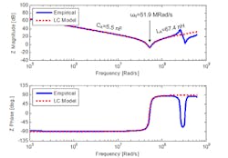
In Fig. 1, an example of an impedance measurement on a SiC module is shown (Lemmon, Graves, 2015a). The plot compares simulated frequency domain data to actual measurement data from a network analyzer with impedance analysis capabilities. The details of the measurement are not important. What is important is the dramatic shift in impedance and phase when the resonant frequency is reached. Understanding this level of detail could be important for an application designer planning to introduce fast edge rates which may excite this resonance (along with other resonances within the application circuit). If this measurement was made with an LCR meter, we would just get a one-dimensional point view at a single far left point of the frequency spectrum. When it comes to GaN power device design, various manufacturers have already wrestled with and addressed the parasitics challenge regarding packaging design. For instance, GaN Systems has developed the innovative chipscale GaNPX packaging and EPC has eliminated the challenge all together by getting rid of the packaging.
From an end-user standpoint when using WBG devices in a power conversion design, the harmonic content generated by the WBG devices combined with unforeseen parastics can lead to power-converter design challenges such as shoot-through and oscillations. Not having the two-dimensional view and insight into the parasitics of the design will typically lead to one of two outcomes for power electronic designers:
- The user will begin to dial the performance of the WBG devices back until the non-ideal behavior stops. This erodes the value proposition of WBG devices by making the WBG device act more like a silicon device.
- The user makes educated guesses on where the parasitics are and tries different parts or various PCB layouts until the problem is gone. This trial-and-error approach significantly increases the design costs and time to market.
Often the real-world picture is a combination of both outcomes—with the end result being that the design takes longer, R&D costs are higher, and the performance is just a bit better than silicon. With design tools that provide two-dimensional insight, this outcome can be avoided. As an example, using software simulation tools that provide field modeling and frequency domain capabilities, users can get a distributed network view into the parasitics of their design across a given frequency range.
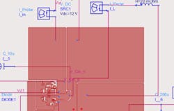
For instance, Keysight Advanced Design System (ADS) Momentum Maxwell field solver takes the layout artwork and PCB or package stackup materials properties and creates an EM-based model of the layout parasitics without having to manufacture the candidate design. The model becomes part of a complete system simulation. This saves on time-consuming, costly, and non-deterministic “solder and see” iterations. Figure 2 shows a “lookalike” symbol from ADS software. The symbol represents the EM-based model of the PCB layout combined with lumped elements to form a complete schematic for ADS Transient Convolution Simulator. By repeating the simulation of various candidate layouts, one can compare output waveforms and avoid problems like power device overstress, oscillation, shoot-through, or other undesirable dynamic behavior.
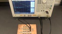
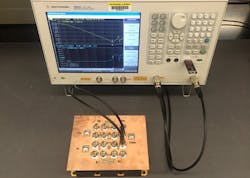
Thus far I have framed up the problem of dealing with WBG design challenges caused by low-level parasitics by simply saying power designers need to adopt two-dimensional analysis tools that are used in the RF world. Of course, there are more layers to the problem than that. Some of the burden or responsibility to make these two-dimensional analysis tools accessible to the power community goes to the makers of the tools themselves. Today, these tools as well as the supporting training material to use them are targeted at the RF community. It is up to the manufacturers of tools to ensure they speak the language of the power designer and meet the form factors of the power hardware. As an example, the blue curve in the Fig. 1 impedance versus frequency plot was made using the setup shown in Fig. 3.
To make an accurate repeatable measurement of low-level parasitics, it is critical to have good fixturing to marry the instrument connections to the device being tested. Without a good interface between the instrument and the device you are analyzing, the parasitics of the interface will dominate the measurement. Manufacturers of these tools provide plenty of high-quality connectors and fixtures for the RF industry to help them make accurate repeatable measurements. But this is not true in the power industry. The fixture shown in Fig. 3 was built by Dr. Andrew Lemmon at the University of Alabama. To build such a fixture to measure the impedance on a SiC power module takes a non-trivial amount of man hours just so you can make the measurement. Whereas if it were an RF device with coaxial connectors, an off-the-shelf fixture could have been easily obtained.
From an industry perspective, there are multiple barriers to WBG device adoption over silicon. Some of the well-known barriers include cost and a proven track record of reliability. Another one that gets less press but affects both manufacturers of WBG devices as well as end users is low-level parasitics in a design. To address this barrier, power designers need to borrow software and hardware design tools from the RF community to look at design parasitics from a two-dimensional impedance versus frequency point of view. At the same time, the makers of these two-dimensional design tools need to ensure there are future versions of these tools that speak the language of the power industry and meet the form-factor needs of their designs.
References:
1.Reusch, David., Strydom, Johan (2013). Understanding the Effect of PCB Layout on Circuit Performance in a High Frequency Gallium Nitride Based Point of Load Converter. IEEE Xplore. Retrieved from: http://ieeexplore.ieee.org/stamp/stamp.jsp?arnumber=6520279
2.Lemmon, Andrew., Graves, Ryan (2015). Parasitic Extraction Procedure for Silicon Carbide Power Modules. IEEE Xplore. Retrieved from: http://ieeexplore.ieee.org/stamp/stamp.jsp?tp=&arnumber=7295986
3.Lemmon, Andrew., Graves, Ryan (2015). Gate Drive Development and Empirical Analysis of 10 kV SiC MOSFET Modules. IEEE Xplore. Retrieved from: http://ieeexplore.ieee.org/stamp/stamp.jsp?tp=&arnumber=7369321
