Solar Cell Combines Two Types of Photovoltaic Material to Produce More Energy
Researchers at MIT and Stanford University have developed a new kind of solar cell that combines two different layers of sunlight-absorbing material in order to harvest a broader range of the sun’s energy. The development could lead to photovoltaic cells that are more efficient than those currently used in solar-power installations, the researchers say (Fig. 1).
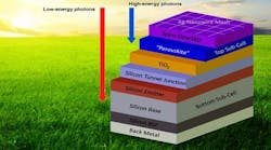
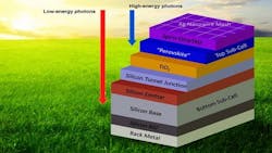
The new cell uses a layer of silicon — which forms the basis for most of today’s solar panels — but adds a semi-transparent layer of a material called perovskite, which can absorb higher-energy particles of light. Unlike an earlier “tandem” solar cell reported by members of the same team earlier this year — in which the two layers were physically stacked, but each had its own separate electrical connections — the new version has both layers connected together as a single device that needs only one control circuit (Fig. 2)
Fig. 1. Test sample of a monolithic perovskite-silicon multijunction solar cell produced by the MIT-Stanford University team. (Image courtesy of Felice Frankel).
The new findings are reported in the journal Applied Physics Lettersby MIT graduate student Jonathan Mailoa; associate professor of mechanical engineering Tonio Buonassisi; Colin Bailie and Michael McGehee at Stanford; and four others.
“Different layers absorb different portions of the sunlight,” Mailoa explains. In the earlier tandem solar cell, the two layers of photovoltaic material could be operated independently of each other and required their own wiring and control circuits, allowing each cell to be tuned independently for optimal performance.
By contrast, the new combined version should be much simpler to make and install, Mailoa says. “It has advantages in terms of simplicity, because it looks and operates just like a single silicon cell,” he says, with only a single electrical control circuit needed.
One tradeoff is that the current produced is limited by the capacity of the lesser of the two layers. Electrical current, Buonassisi explains, can be thought of as analogous to the volume of water passing through a pipe, which is limited by the diameter of the pipe: If you connect two lengths of pipe of different diameters, one after the other, “the amount of water is limited by the narrowest pipe,” he says. Combining two solar cell layers in series has the same limiting effect on current.
To address that limitation, the team aims to match the current output of the two layers as precisely as possible. In this proof-of-concept solar cell, this means the total power output is about the same as that of conventional solar cells; the team is now working to optimize that output.
Fig. 2. Schematic diagram shows the layered structure of the hybrid solar cell. The top sub-cell, made of pervoskite (blue), absorbs most of the high-energy (blue arrow) photons from the sun, while letting lower energy (red arrow) photons pass through, where they are absorbed by the lower sub-cell made of silicon (gray).
Perovskites have been studied for potential electronic uses including solar cells, but this is the first time they have been successfully paired with silicon cells in this configuration, a feat that posed numerous technical challenges. Now the team is focusing on increasing the power efficiency — the percentage of sunlight’s energy that gets converted to electricity — that is possible from the combined cell. In this initial version, the efficiency is 13.7 percent, but the researchers say they have identified low-cost ways of improving this to about 30 percent — a substantial improvement over today’s commercial silicon-based solar cells — and they say this technology could ultimately achieve a power efficiency of more than 35 percent.
They will also explore how to easily manufacture the new type of device, but Buonassisi says that should be relatively straightforward, since the materials lend themselves to being made through methods very similar to conventional silicon-cell manufacturing.
One hurdle is making the material durable enough to be commercially viable: The perovskite material degrades quickly in open air, so it either needs to be modified to improve its inherent durability or encapsulated to prevent exposure to air — without adding significantly to manufacturing costs and without degrading performance.
This exact formulation may not turn out to be the most advantageous for better solar cells, Buonassisi says, but is one of several pathways worth exploring. “Our job at this point is to provide options to the world,” he says. “The market will select among them.”
“I think this work is very significant,” says Martin Green, a professor at the University of New South Wales, in Australia, who was not connected with this research. “The work is important in establishing a proof-of-concept and will stimulate higher efficiencies with this approach. … It’s an excellent starting point for further work in this area.”
The research team also included Eric Johlin PhD ’14 and postdoc Austin Akey at MIT, and Eric Hoke and William Nguyen of Stanford. It was supported by the Bay Area Photovoltaic Consortium and the U.S. Department of Energy.


