How to Design an Optimal Electronic Load for High-Current, Low-Voltage Power Supplies (Part 3)
Download this article in PDF format.
The design challenges for a high-power electronic load extend beyond the electronics. The best electronic load circuit will not function well without a good connection to the device under test. The connection should be easy to make and break, have extremely low electrical resistance, and minimize the physical path length for the current. Keeping the high-current path short and small in area reduces parasitic inductance that’s detrimental to the load current slew-rate performance.
What’s the Best Connector?
Through-hole connectors are advantageous because they can connect to all copper layers in both the load and supply PCBs. The more through-hole pins per contact, the better, because the current can enter and exit the PCBs at more points, reducing resistance. In addition, the through-hole connection is physically very robust, which is important for a load device that will be in service through many hundreds of connection cycles.
Press-fit connectors can further reduce resistance by eliminating the solder junctions between the PCB through-hole and the connector pins. Solder is a comparatively poor conductor versus copper, at about eight times higher volume resistivity. A press-fit connection forms a direct electrical junction between the pin and PCB copper.
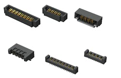
The Samtec UPS and UPT series of connectors is an excellent choice. They’re able to handle very high current in a small form factor. Connectors in this series are available with vertical and horizontal orientation. Pin counts range from two to eight. An example of the 8-pin version is shown in Figure 1.
Each mated contact pair (male and female) presents a resistance of about 300 µΩ. The effective thermal resistance is about 200°C/W, and typical contact temperature rise above ambient is about 40°C with no airflow for an 8-pin connector pair with 100-A current (100 A to the load and 100 A returning to the supply ground). Because the UPS and UPT right-angle connectors have an open, flow-through design, exhaust airflow from the electronic load fan also cools the connector as a side benefit.
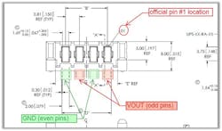
It’s important to interleave power and ground connections as shown in the example in Figure 2 to minimize the magnetic loop area in the connection. This, in turn, minimizes parasitic inductance.
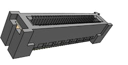
Another good option for smaller load devices is a connector that can accept a bare “card edge.” The connector can reside on the load or the device under test, and the mating device is constructed with exposed copper on the top and bottom at one edge. The Samtec HSEC8-130-01-S-DV-A-WT-TR connector in Figure 3 is a good example of a card-edge socket; it accepts a 0.062 in. PCB that’s 0.994 in. wide.
Regardless of the connector chosen, it’s important to coordinate design efforts so that both the power supply to be tested and the electronic load are built with mating connectors, placed carefully to avoid mechanical obstructions that would prevent connection.
When to Use a Heatsink
An electronic load that’s intended solely for testing transient response can be designed without a heatsink, provided that operating duty cycle is kept very low. However, an electronic load that’s intended to test supply efficiency will almost certainly require a heatsink.
An aluminum heatsink with a cooling fan can drastically lower the effective thermal resistance of the power components, raising the power-handling ability of the design tenfold from a PCB with no airflow. Sinks with fins will perform well for natural convection, but “pin-fin” sinks typically work better when combined with a fan.
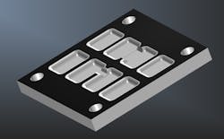
Pin-fin heatsinks are readily available in a wide range of sizes and configurations. Most sinks will have a flat mating surface, but this can be easily customized to more closely fit the MOSFETs and sense resistors. For instance, Front Panel Express LLC provides a simple freeware CAD tool that can be used to define pockets to be machined into an aluminum panel, allowing for precise clearances between the heatsink mating surface and the components to be cooled.
An example of this is shown in Figure 4, where the mating face of a standard 40-mm BGA heatsink is machined to clear four MOSFET and sense resistor pairs. In addition, mounting screw holes are drilled through the sink, facilitating attachment to the PCB and fan.
Thermal Interface Options
To obtain the best thermal connection between the power components and the heatsink, some thermal interface material is required. Many options exist, from pastes to flexible sheets. The thermal conductivity is a property of the material chosen, and thermal resistance varies with the thickness. Accordingly, the thickness of the interface material layer between the components and the heatsink should be minimized, regardless of the interface material type.
Choose a material that presents a good tradeoff between ease-of-handling and rework, with high thermal conductivity. Also, select a material with physical conformance characteristics that will allow it to form or flow into thin sections without exerting high forces on the PCB and components.
Thermal conductivity k will typically be given in units of W/mK. Higher values are better. The thermal resistance varies proportionally with the thickness of the interface, and inversely with the area of the mating surface.
Θ = L / (k x A)
For example, consider a 10-mil layer of Laird Technologies’ Tcpm 580 phase-change interface material, placed between a 5- × 6-mm MOSFET case and the heatsink. The interface material thermal conductivity is 3.8 W/mK, so the thermal resistance is as follows:
Area: A = 5 mm × 6 mm = 30 mm2 = 0.00003 m2
Thickness: L = 0.010 in. × 0.0254 m/in. = 0.000254 m
1K = 1°C
ΘCS = (0.000254 m) / (3.8 W/mK × 0.00003 m2) = 2.22°C/W
Now let’s consider a PSMN2R0-30YLE power MOSFET that carries a load current of 25 A at a voltage drop of 0.675 V, dissipating 16.875 W (Fig. 5).
We would expect to see a junction temperature rise above the heatsink temperature according to the following:
TJ = Power × (ΘJC + ΘCS)
TJ = (25A x 0.675V) × (0.45°C/W + 2.22°C/W)
TJ = 16.875W × 2.67°C/W = 45.1°C
So, to maintain the junction temperature below the maximum limit of 175°C, the heatsink mating face must not exceed 129.9°C.
Similar analysis applies to the sense resistors, with the exception that there generally isn’t an equivalent parameter for junction-to-case thermal resistance. In most high-power sense resistor construction, the resistive element and the case are essentially the same, so only the case-to-sink thermal resistance is needed.
In addition to thermal conductivity, the electrical conductivity of the interface material must also be considered. In most applications, an electrically insulating material is required because the interface will be in direct contact with exposed surface-mount pads and pins on the MOSFETs and sense resistors. This generally precludes use of some otherwise highly thermally conductive materials, such as graphite.
Layout and Floorplan Guidance
Many “off-the-shelf” heatsinks and aluminum extrusions are readily available. In fact, selecting the heatsink before beginning the PCB layout can guide many decisions about placement of the power transistors and sense resistors. Allowances should be made for all of the following mechanical necessities:
- Power MOSFETs
- Sense resistors
- Heatsink and fan mounting screw locations, including mounting hardware (threaded standoffs or other anchors)
- Temperature-sensing ICs or passive components; e.g. thermistor or resistive temperature detector (RTD)
- Power connector
In general, only place power components on the heatsink surface of the PCB, and place non-power devices and passives on the reverse side, or outside the area covered by the heatsink. This keeps peripheral components away from the hottest area of the PCB and simplifies any necessary customization of the heatsink mating face. Evenly distributing the power components will create a more uniform power-density profile, reducing local hotspots.
The conducting path should be as wide and as direct as possible. The load current flows through PCB copper from the supply pins of the connector to the MOSFET drain, from the MOSFET source to the high side of the sense resistor, and finally from the sense-resistor low side back to the ground pins of the connector. Ideally, the PCB layout should include polygons or planes on multiple layers, with stitching vias, to provide the lowest resistance connection between these points. Careful floorplanning of component placement can greatly improve the overall performance, as well as simplify PCB trace routing.
Cooling the Heatsink
For a high-power electronic load with a compact form-factor, radiative and natural-convection cooling will generally be inadequate to remove heat. Forced-air cooling with a fan is the most effective cooling technique, short of liquid cooling.
Forced-Convection Cooling with a Fan
Selection of a heatsink for use with a fan favors thicker fins or pins, with narrower spacing, compared to a natural convection heatsink. A general rule of thumb is that pins or fins should be 2 mm thick or more, with at least two or three fins per centimeter, or least six pins per square centimeter. At the upper limit, high fin or pin density and narrow spacing will restrict airflow, so it’s important to maintain a reasonable balance between density and airflow restriction.
Because radiative cooling is only a small contributor to overall heat flow when forced-convection cooling is used, surface treatment isn’t critical. Anodized or coated heatsinks have better emissivity, but they will not perform markedly better than bare metal in forced-convection applications.
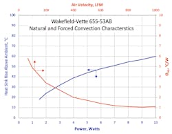
Suitable heatsinks will typically be provided with thermal performance data (Fig. 6). Shown are both the thermal resistance as a function of airflow and the temperature rise as a function of power, for the Wakefield-Vette 655-53AB heatsinks.
If the 655-53AB heatsink is paired with a high-performance 40-mm fan, we can determine the approximate thermal performance by combining the fan’s volumetric flow rate with the cross-sectional area of the flow path.
Consider the 40-mm square Wakefield-Vette heatsink 655-53AB cooled by a Sanyo-Denki 9GE0412P3K03 fan, mounted atop the sink. The air enters the top of the pin-fin sink and exits through the sides. Each of the four outlet sides has an approximate open area of about 1.6 by 0.375 in., which gives a total unobstructed exit area of about 2 in.2, or about 0.015 square feet.
The fan generates a nominal 26.8 cubic feet per minute (CFM) of airflow. To obtain the equivalent flow velocity in linear feet per minute (LFM), we divide the CFM value by the area of the flow path. This yields an airflow velocity of almost 2000 LFM. Actual flow will be considerably less due to significant “wind resistance” in the convoluted flow path through the heatsink pins. If we derate the airflow by 55%, that yields a linear flow of about 900 LFM.
Figure 6 shows that the 655-53AB heatsink will exhibit a thermal resistance ΘHS of about 1.0°C/W at 900 LFM. Earlier, we found that the heatsink mating surface for our hypothetical design must remain below 129.9°C. If the ambient air temperature is 25°C, our fan-cooled heatsink is adequate for a total continuous electronic-load power dissipation up to 104.9 W.
Peak transient power levels can greatly exceed the continuous power capability because the combination of the component packages, PCB, and heatsink has considerable thermal capacity. This thermal capacity contributes to a fairly long thermal time constant.
Analogous to a current source driving a chain of resistors and capacitors where current leads voltages, the load power dissipation is a thermal flux that drives the chain of thermal resistances and capacitances. Temperatures will lag behind the thermal flux; low thermal resistances and large heat capacities will reduce the temperature rise at each junction for time-limited power pulses.
Electronic Fan Speed Control
In most cases, the electronic load will not operate at full power all of the time. In fact, operation at maximum power tends to be very brief. Therefore, the cooling fan needn’t be operated at maximum speed all the time.
There are many active fan-controller ICs available to adjust the fan speed based on the PCB temperature. For example, Maxim’s MAX31740 provides a pulse-width-modulated (PWM) control signal that varies with the temperature measured by a small, low-cost negative temperature-coefficient (NTC) thermistor. If the thermistor is placed near the physical junction of the power components and the heatsink, the cooling fan speed will vary with the power dissipation in the load.
This provides ergonomic benefits by reducing the fan noise when the load is at low power or idle, while also delivering audible feedback to the operator when the load power is high and the heatsink is hot. The reduced fan speed at low power also lowers the power consumption of the load itself and maximizes the useful service life of the fan.
More sophisticated fan-controller ICs provide digital telemetry for the load temperature and can detect fan-motor failure, allowing the load to shut down automatically before it’s damaged by excessive heat.
Water Cooling
The effectiveness of forced-air cooling is limited by tradeoffs between the heatsink surface area exposed to airflow and the conductive flow path between the mating face and the cooled surfaces. Increasing the ratio of air-cooled surface area to mating face area tends to either increase the length or reduce the cross-section of the conductive path. At some point, reductions in the convective thermal resistance are offset by increased conductive thermal resistance, and the heatsink performance suffers.
One way to get around this constraint is to introduce a fluid heat-transfer medium, which can mechanically transport thermal energy from a heat-source with small contact area to a radiator with large area. This will break the conductive heat-transfer bottleneck that limits traditional heatsink performance.
Of course, liquid cooling greatly increases the complexity of the electronic-load design, and presents considerably more issues with maintenance, portability, and overall reliability. However, at very high power, it may be the only viable option.
Thanks to advances in liquid-cooling technology for personal computers, it’s possible to adapt off-the-shelf radiators, pumps, and water blocks for use in an electronic load.
Overpower Protection
The electronic load can be protected against high temperature and excessive power dissipation in several ways. The simplest protection is to compare the current measurement against a fixed threshold. If the threshold is exceeded, the circuit shuts off the control signal or otherwise disables the current-sink circuit. This prevents further temperature rise, thus protecting the components in the load.
Such protection can be improved by using a threshold that falls with rising temperature. For instance, it can be achieved by using a temperature sensor IC which outputs a voltage that decreases linearly with temperature.
The drawback of simple overcurrent protection is that current isn’t proportional to power if the VDUT voltage changes. At higher voltages, the same current represents considerably higher total power in the load. Direct measurement of power can be implemented by adding an analog multiplier to generate a power signal from the product of voltage and current.
When protection is invoked, a latching comparator should be used, enabling the load to cool down before further operation. The operator can then reset the load after reducing the power demand. Alternatively, the device can be designed to automatically restart when the temperature drops to a safe level.
Conclusion
Implementing a useful electronic load for testing high-current, low-voltage supplies requires careful consideration of not only the circuit design, but also the thermal and mechanical construction. Following the guidelines and principles outlined in this article will ensure the load can operate at high power while maintaining good performance and reliability.
Dwight Larson is Principal Member of the Technical Staff, Cloud & Data Center Business Unit, at Maxim Integrated.
References
Chroma application note: “Selecting Electronic Loads for Low Voltage High Current Applications”
Chroma Electronic Load datasheet: Model 63640-80-80
Wakefield-Vette application note: “Heat Sink Design Facts and Guidelines for Thermal Analysis”
Nexperia AN11599: “Using Power MOSFETs in Parallel”
Nexperia datasheet: PSMN2R0-30YLE
Vishay-Dale datasheet: WSL3627 Power Metal Strip® Resistors

