Designing a High-Power LLC Resonant Half-Bridge DC-DC Converter
Download this article in PDF format.
The quest for higher power and greater efficiency in all power supplies never ends, especially when it comes to all heavy-duty converters. Some examples are power supplies used in data centers, telecom facilities, industrial automation, solar inverters, and automotive battery chargers.
In such cases, dc-dc converters are typically the prime target. Currently multiple designs exist. As a designer, you’re probably tempted to take the traditional design route. But what if you found out about an alternative approach combining a unique power circuit and a microcontroller (MCU) that could deliver a truly improved product? You just may want to consider this approach.
Sponsored Resources:
- Scaling real-time control resources to meet performance demands
- Design a resonant converter using C2000™ real-time controllers
- What other advantages can C2000™ MCUs provide to your power electronic design?
An LLC Resonant Converter
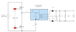
A good starting point for a high-power dc-dc converter design is to use a LLC resonant half-bridge circuit. The basic circuit is shown in Figure 1. The input is dc in the 400-V range, which was probably derived from a power-factor-correction (PFC) circuit. This input dc is then applied to the half bridge.
Gate-drive pulses switch the half-bridge MOSFETs with a 50% duty cycle. The resulting square wave is applied to the primary winding of a transformer. The transformer usually steps the voltage down. Switching frequency is typically in the 200- to 350-kHz range.
The transformer’s primary winding is part of a series-resonant circuit made up of the capacitor C and two inductances—the transformer magnetizing inductance Lm and an external series-resonant inductor Lr. The two inductances add up to a value of Ls:
Ls = Lr + Lm
The resulting resonant frequency is:
f = 1/2π√(LsC)
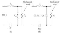
The equivalent circuit in Figure 2a reveals that the resulting series circuit includes a resistance of RL. This is the output load resistance and rectifier resistances reflected by the transformer secondary back into the primary. At resonance, in the series circuit, the inductive reactance cancels the capacitive reactance. Therefore, the load as seen by the half bridge is only that reflected load resistance.
The equivalent circuit indicates that two resonant frequencies are possible, one with C and Lr and the other one with Lm and C. Only the more dominant inductor is recognized, and this resonant circuit is employed for regulation and power control. The LLC series circuit used in this discussion is typical, but you should know that another option is to utilize two capacitors (LCC) instead of two inductors (Fig. 2b).
An important consideration is that the series-resonant circuit acts as a filter to eliminate the upper harmonics from the square wave, making the voltage on the transformer a sine wave. The rectifier on the secondary transforms the sine wave into the desired dc output.
To control the output, the frequency of the signal driving the half-bridge is varied. The gate-drive circuits vary their frequency over a narrow range while maintaining a 50% duty cycle. Guard bands between the positive and negative pulses provide a zero-voltage-switching (ZVS) transition. Peak power is delivered at the point of resonance. Changing the drive frequency above or below resonance will maintain the output voltage at the desired level.
The real need in this design is a source for those variable-frequency gate-drive signals. The most logical source is the main MCU. Most MCU controllers provide pulse-width-modulation (PWM) control of duty cycle to implement switching power supplies. The proposed system uses variable frequency to adjust the output; the MCU can hold the PWM outputs to 50-50%.
For some applications, the half-bridge circuit may not provide enough output. In that case, two of the half-bridge/LLC/rectifier circuits of Figure 1 can be combined by putting their inputs and outputs in parallel and using complementary gate drives on the two half-bridges. Such an arrangement will deliver the extra power. In this case, a current-sharing arrangement is needed to prevent one circuit from interfering with and degrading the other.
Incidentally, a reference design for a two-phase interleaved LLC resonant converter using the C2000 is available from TI. Check out this reference design using the newest C2000 real-time control MCUs.
The C2000 MCU Targets Real-Time Control and Power Conversion
Hundreds of different MCUs are available to implement switch-mode supplies. Yet very few are proficient at real-time (RT) control. Real-time control implies that the MCU must be able to meet the timing needs of the external device it’s controlling or monitoring. It’s also expected the MCU will be fast enough to carry out processing between these critical timing points.
In addition, many RT applications require the use of complex mathematical algorithms that can be executed in a timely manner if a specific external event occurs. Then the MCU must be ready for other demanding time restrictions.
An RT MCU also benefits from having some of these features:
- 32-bit floating-point processor
- Precision PWM
- On-board DAC
- On-board ADCs
- Comparators
- Multiple interfaces (CAN, Ethernet, EtherCAT, SPI, I2C, UART, USB 2.0)
- Configurable logic blocks (LUTs)
- Many GPIOs
Another important requirement is scaling the real-time control resources to meet performance demands. This can be manifested by a distributed architecture design that involves devoting an MCU to each major function, and then interconnecting and synchronizing them via a fast serial bus.
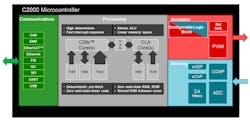
One MCU with all of those unique features is Texas Instruments’ C2000. Figure 3 summarizes the main content. Check out the C2000 Key Technology Guide to see the many technologies, features, and peripherals within C2000 MCUs and how you can take advantage of them within your design.
Sponsored Resources:


