This Week in PowerBites: Are QJTs Real?, Smart LED Drivers
>> Electronic Design Resources
.. >> Library: Article Series
.. .. >> Article Series: PowerBites
Advanced Micro-Trench IGBTs Now Comes in a TO-247 Housing
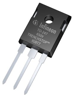
Infineon Technologies’ TRENCHSTOP IGBT7 technology is now available in a discrete housing: a TO-247 with 650-V breakdown voltage. The new TRENCHSTOP family portfolio has current ratings of 20, 30, 40, 50, and 75 A. It can easily replace previous technologies and be used for paralleling. This version of IGBT7 is especially suited to applications such as industrial motor drives, power factor correction, photovoltaics, and uninterruptible power supplies.
Fabricated using the company’s new micro-pattern trench technology, the TRENCHSTOP IGBT7 chip operates with significantly lower static losses than previous comparable devices. For the same current class, the on-state voltage drop is reduced by 10%. This feature brings significant loss reduction in the application, especially for industrial drives, which usually operate at moderate switching frequencies.
The IGBT T7 technology also produces devices with very low saturation voltage (VCE(sat)), which can be co-packed with an emitter-controlled 7th-generation (EC7) diode. The combination provides for a 150-mV lower forward voltage (VF) drop and improved reverse-recovery softness.
The device features superior controllability and excellent EMI performance. As a result, it can be easily adjusted to provide the best ratio of dV/dt and switching losses for each application. The 650-V TRENCHSTOP IGBT7 passed the JEDEC-based HV-H3TRB (High Humidity, High Temperature and High Voltage Reverse Bias) test, making it suitable for use in high-humidity environments, such as those often be found in industrial applications.
The discrete TRENCHSTOP IGBT7 can be ordered now; devices are available through distribution (and samples from Infineon). Visit this page for further data (including links to pricing information); https://www.infineon.com/cms/en/product/power/igbt/trenchstop-igbt7/?redirId=64262#!products.
LED Drivers Optimized for UHD TV Backlight Units
MagnaChip Semiconductor Corp. announced two new LED driver ICs for UHD TV BLUs (backlight units). The 1- and 2-channel devices were developed to address the needs of UHDs used in mid-range HDTVs. They deliver consistent lighting across the LED display panel, as well as enable the BLU to adjust ambient light settings and generate a consistent image quality.
Both drivers feature higher contrast ratio and improved power efficiency thanks to a hybrid dimming circuit, which combines the best aspects of analog and pulse-width-modulation (PWM) dimming technologies. The drivers also incorporate important circuit-protection functions including short-circuit protection, undervoltage lockout, over-duty protection, current-sense resistor short protection, and drain-source short protection. With these protection features, the main circuit can supply consistent power and prevent a short circuit even under varying electrical flow conditions. Please visit www.magnachip.com for more information.
Smart LED Driver Combines PFC with GaN Power Switch for 90%+ Efficiency
The LYT6078C, a new member of Power Integrations’ LYTSwitch-6 family of safety-isolated LED drivers for smart lighting applications, integrates a PFC fabricated in silicon and a LYTSwitch-6 LED driver 750-V power switch based on the company’s PowiGaN gallium-nitride (GaN) technology. Together, they enable the smart LED driver to deliver flicker-free output up to 90 W with over 90% efficiency.
Housed in a miniature InSOP-24 surface-mount package, LYTSwitch-6 ICs are protected by an advanced thermal foldback system. The system reduces output power to limit device temperature during abnormal conditions, while still providing light output. All devices in the LYTSwitch-6 family also incorporate Power Integrations’ FluxLink communication technology. FluxLink allows for secondary-side control without the need for an optocoupler and provides better than ±3% CV and CC regulation across line, load, temperature, and manufacturing. All LYTSwitch-6 ICs exhibit fast transient response and easily support PWM dimming.
The performance benefits of the LYT6078C are documented in the design report DER-920, which details a reference design for a two-stage PFC boost plus isolated flyback on a dimmable LED ballast based on the LYTSwitch-6 LYT6078C and the HiperPFS-4 PFS7624C PFC controller. The design provides peak efficiency of greater than 91% when driving a 48-V LED string at 1350 mA from a 220- to 277-V ac input. In standby mode, system power consumption is less than 80 mW, giving engineers substantial flexibility when designing lighting controls and particularly dim-to-off circuits.
PowiGaN-based LYTSwitch-6 LED-driver ICs are available now, priced at $2.52 in 10,000-unit lots. For technical support and the DER-920 design report, visit Power Integrations’ website at https://www.power.com/lytswitch-6/.
DC-DC Buck-Boost Converter Offers Super-Low IQ, Extends Battery Life by 50%
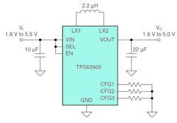
According to Texas Instruments (TI), it has introduced the industry’s first dc-dc buck-boost converter to combine programmable input current limit and integrated dynamic voltage scaling to extend battery life by at least 50%. The company says the TPS63900 maintains the industry’s lowest quiescent current (IQ)—75 nA—with 92% efficiency at 10 µA and delivers up to three times more output current than competing devices to help engineers extend the lifespan of battery-powered industrial and personal electronics applications.
The TPS63900 was designed specifically to help engineers conserve energy in battery-powered applications that rely on wireless technologies such as narrowband Internet of Things (IoT), Bluetooth (Low Energy, and long range), and wireless M-Bus. It does this by integrating dynamic voltage scaling to deliver power while keeping the system at the minimum voltage required to operate efficiently, maximizing battery life and reducing required maintenance for industrial applications.
With such a feature, design engineers can optimize power architectures for ultra-low-power sensors and wireless connectivity integrated circuits. It supports applications that can operate for at least 10 years using the primary battery.
The TPS63900 also efficiently charges supercapacitors to buffer peak loads, protect battery capacity, and extend system lifetime and performance. Fully charged supercapacitors help buffer the energy required to operate components that require high peak currents, such as those found in motorized smart locks.
For more details, and to see how an integrated programmable input current limit reduces bill of materials and total solution cost, see the application note, “Using input current limiting to extend battery life.” The buck-boost converter can also be paired with TI’s MSP430FR2155 in security sensors or wireless IoT sensors to monitor the vibration of water pumps for predictive maintenance and help drive down costs. To learn more, read “5 best practices to extend battery life in flow meters.”
The TPS63900 is now available through TI and authorized distributors in a 2.5- × 2.5-mm wafer small-outline no-lead (WSON) package. Pricing is US$0.80 in 1,000-unit quantities. Full and custom quantity reels are available on TI.com and through other channels. Also, go to the website for the TPS63900EVM evaluation module (US$49).
Current-Compensated Dual-Choke Filter Inductors are AEC-Q200-Compliant
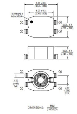
Bourns Inc. recently unveiled its Model DR334A Line Filter Series of current-compensated dual-choke filter inductors. They feature higher current capability than typical standard signal-line common-mode chokes, as well as high stray inductance and differential-mode noise rejection. These capabilities make the DR334A series well-suited for line filter solutions targeting consumer, industrial, and other market power-line applications, or in applications where power is transferred across signal lines, such as power over Ethernet (PoE) systems.
The new Model DR334A series is available in a bifilar-wound configuration to reach higher common-mode impedance, and a sector-wound configuration to reach higher differential-mode impedance at high frequencies. Offered in a compact, low-profile (height 3.6 mm) size and in a broad range of inductance ratings from 11 µH up to 4700 µH, Model DR334A line filters enable designers to set the filter curve best suited to their application. All components in the series are AEC-Q200-compliant with an extended operating temperature range of −40 to +135°C and a rated voltage up to 80 V dc. In addition, their closed and ferrite toroid core construction delivers a more efficient and robust mechanical design.
The RoHS-compliant and halogen-free DR334A Line Filter Series is available now. More detailed information can be found at https://www.bourns.com/products/magnetic-products/common-mode-chokes-aec-q200-compliant
First Tests of Quantum-Junction Power Transistors Look Promising
The term "quantum junction transistors” (QJTs) may conjure images of dilithium crystals, flux capacitors, and other imaginary power technologies, but an early demonstration run of Nottingham-based Search For The Next's (SFN) unique "Bizen" wafer process technology has moved the devices from the realm of science fiction to science fact. In fact, SFN says that the results were so promising that, if Bizen can replicate the results in its production devices, they should pose some very real competition to conventional silicon and WBG power devices.
In case you missed the introduction to SFN's QJT technology we published back in June 2020, the process referred to as “Bizen” is based on the principles of quantum-tunnel mechanics and, according to SFN, can be used to dramatically improve the performance and producibility of any digital or analog semiconductor device. Since our article ran, those claims were validated when SFN produced and evaluated an undisclosed number of wafers containing QJT devices.
At the time of this writing, details of the wafer tests weren’t available, but the company said that the data they collected demonstrated the silicon-based transistors deliver the same voltage levels, switching speeds, and power-handling performance normally associated with devices fabricated using more exotic wide-bandgap materials. The wafer tests also show that the Bizen process can use conventional silicon wafers to produce QJTs that support operating voltages of up to 1200 V, very low conductive losses, and an effective current gain of over 1 million.
SFN's Bizen process also has some additional unique advantages, including the ability to efficiently support low-voltage digital logic on the same chip as high-power transistors. Additional details on this, and QJT technology's potential impact on conventional devices are covered in this feature story published last week.
>> Electronic Design Resources
.. >> Library: Article Series
.. .. >> Article Series: PowerBites


