How SiC Transistors Can Improve Power-Conversion Efficiency
What you'll learn:
- Properties of wide-bandgap materials, with a focus on SiC.
- How a bridgeless totem-pole topology can help cut losses.
- A breakdown of the half-bridge inverter topology
The efficiency of power-conversion systems is getting attention and becoming increasingly important for economic and environmental concerns. The efficiency levels defined in the 80 PLUS standard class Titanium require up to 96% (at 50% load): alternative, more efficient topologies and the adoption of transistors based on wide-bandgap (WBG) materials can help minimize the overall losses, thus improving the efficiency.
This article aims to show the benefits of using SiC MOSFETs as an alternative to more traditional power switches in some areas of power conversion. We start with an overview of WBG materials and describe how their characteristics influence the main parameters of the power transistor and its features and behavior in practical applications.
Emphasis is given to the improvement in efficiency that’s achievable with SiC transistors. For this purpose, we show two main examples: the totem-pole bridgeless PFC topology, and a half-bridge inverter. These topologies can be used in wide variety of applications ranging from motor control to uninterruptible power supplies and renewable-energy generation systems. We analyze the examples for power losses and present results.
Introduction to WBG materials
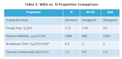
WBG materials feature a relatively wider energy bandgap (between the valence band and conduction band) compared to conventional silicon. Silicon carbide (SiC) and gallium nitride (GaN) are the most popular WBG materials in use today. Table 1 shows the main characteristics of WBG and Si-based materials.
Many material compounds exist in different crystal structures called polymorphs. SiC is quite unique in this regard as researchers have identified more than 250 different SiC polymorphs. The 3C-SiC and 4H-SiC are the most used polytypes thanks to their superior semiconductor properties. SiC transistors used for this article are 4H-SiC based.
The energy gap expressed in eV is the difference between the bottom of the conduction band and the top of the valence band of the electrons in a crystalline solid. Semiconductors exhibit a 1 eV < EG < 4 eV, while materials with an EG above 9 eV are generally insulators and those with an EG below 1 eV are conductors.
The electron mobility is a measure on how quickly an electron can move through the material when subjected to an electric field. The higher energy gap and the lower electron mobility shown by the SiC MOSFET versus a Si-based MOSFET (Table 1, again) affects the channel resistance: i.e., SiC MOSFETs have a higher channel resistance than Si MOSFETs, thus a higher input voltage is usually required to properly saturate a SiC MOSFET.
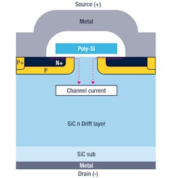
On the other hand, the higher energy gap means that SiC MOSFETs exhibit lower leakage current variation with temperature. The operating temperature of SiC MOSFETs is also much higher and limited by reliability considerations related to the package. The on-resistance exhibited by high-voltage MOSFETs is mainly due to their thickness and the resistivity of the drift layer (Fig. 1).
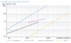
The breakdown field of SiC MOSFETs is 10 times higher than that of silicon. Consequently, at parity of breakdown voltage, a lower resistivity and thickness are required for the drift layer due to the SiC MOSFET’s extremely low RDSon as compared to Si-based MOSFETs. Figure 2 shows the theoretical limit of on-resistance per area for WBG and Si-based transistors.
While currently available Si-based transistors are close to their Ron * Area limit, the technology for producing SiC devices is still in the early stage of its learning curve. Therefore, we can expect to see improved performance in future generations.
It’s worth noting that, for a given on-resistance and breakdown voltage, a SiC MOSFET requires significantly less die area than a conventional silicon MOSFET. Thus, it will have smaller capacitances and lower gate charge, which translate into lower switching losses and greater efficiency.
The higher thermal conductivity reflects as a lower thermal resistance. At parity of area, SiC MOSFETs show much lower thermal resistance, leading to a lower working junction temperature.
SiC Transistor in Its Environment
Despite all of the benefits previously described, the previously high cost of SiC transistors had limited their use to specialized applications in high-end industrial markets (e.g., oil drilling power supplies, military power systems, etc.). Major factors influencing their cost had been attributed to factors such as the higher cost and lower availability of SiC substrates, the higher cost of SiC manufacturing processes, and lower production yields (mainly due to higher defect densities of the substrates).
More recently, advances made in the quality of the substrates have resulted in significant improvements in the yield and reliability of SiC devices. This, and greater availability of substrates has dramatically enhanced the efficiency and manufacturing cost of these transistors, encouraging their broader adoption in electric-vehicle systems such as on-board chargers and traction inverters.
With SiC transistors enabling more efficient and higher switching frequency and consequently reducing the size of the magnetic components, WBG material is driving the adoption of SiC in many sectors of power conversion in the industrial market—on top of the gains it’s made in automotive applications.
But SiC doesn’t belong everywhere. The success of IGBTs in renewable-energy systems, UPS, and motor controllers is largely due to their small conduction losses and the relatively low switching frequencies required by these applications. IGBTs can be produced in different families by changing the tradeoff VCE(SAT)-tfall and thus optimizing the conduction losses versus the switching losses.
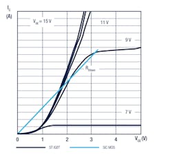
However, paralleling several IGBTs changes the slope of the output characteristic. On one hand, the ON voltage will never be lower than the voltage offset established by the knee effect of the IGBT (~0.8V). On the other hand, paralleling “n” MOSFETs results in dividing the RDS(on) of the single MOSFETs by “n,” thus achieving the lowest possible conduction losses (Fig. 3).
In practical applications, it is possible to exploit that characteristic without necessarily achieving the lowest conduction losses in all conditions. Some motor-control applications, such as the inverter for an electric car or a compressor for refrigeration, operate for most of their life at a fraction of their nominal power (between 20% and 50% of full load). So, even here, the adoption of SiC transistors allows for lower losses and higher efficiency (Fig. 3, again).
Totem-Pole PFC
We already mentioned that energy losses in many areas of power conversion can pose serious economic and environmental concerns. For this reason, an efficient power-factor-correction (PFC) stage between the rectification stage made by the low-frequency input bridge and the following dc-dc converter can help to reduce the total losses.
In many cases, achieving the required efficiency requires minimizing the losses in each of the three stages of the power supply. Bridgeless topologies can help by eliminating the losses on the input stage and therefore contribute to reaching the targeted efficiency level.
The PFC totem-pole bridgeless topology is well known in literature, though losses due to the high recovery of the intrinsic body diode of the MOSFETs basically limit its use to discontinuous-conduction-mode operation and, thus, mainly low power applications. On the other hand, with negligible reverse-recovery current of the intrinsic body drain diode, SiC transistors give new perspective to this topology.
Figure 4 shows the bridgeless PFC totem pole (left) and the semi-bridgeless totem-pole PFC topology (right). The semi-bridgeless topology uses two thyristors to limit inrush currents, replacing the typical circuit that uses a less-efficient current-limiting resistor and relay to perform the function.
In a conventional PFC topology, there are two bridge diode voltage drops and one drop at the boost stage, while in the totem-pole bridgeless topology, two low-resistance MOSFETs in the low-frequency leg of the bridge eliminate diode drop and improve the efficiency. In addition, the totem-pole bridgeless PFC minimizes power loss in the conduction path.
As shown in Figure 4, the totem-pole topology consists of two SiC MOSFETs (S1, S2) operating at a high switching frequency, typically between 65 and 150 kHz, and a pair of low-resistance MOSFETs (M1, M2) operating at line frequency (47 ~ 63 Hz). The conduction path includes only one fast switch and one slow switch.
The low-frequency MOSFETs can be replaced by two thyristors, providing a useful advantage to control inrush current at startup, replacing the relay and inrush resistor used in earlier designs. This solution offers interesting advantages in reliability while reducing standby losses compared to the traditional NTC/PTC inrush-current limitation.
In the high-frequency leg, the very small reverse-recovery charge of SiC MOSFETs compared to silicon MOSFETs also makes the totem-pole bridgeless PFC practical for high-power applications. It meets the demand of UPS and motor-control applications by achieving very high efficiency and high power density.
Table 2 shows the calculated efficiency for a PFC semi-bridgeless topology that uses two thyristors and two SiC MOSFETs. For this example, we will use TN5050H-12WY thyristors and STCW90N65G2V SiC MOSFET devices. The SiC FETs have a maximum RDSon of 24 mΩ at 25°C and are driven with positive and negative gate voltage (+20 V, −4 V) using a galvanically isolated, half-bridge dual-channel gate driver with 4-A sink/source current capability (STGAP2D). Table 2 was built with calculations done for different input voltage and power levels, assuming a dc bus voltage of 400 V dc and a switching frequency of 100 kHz.
The analysis is based on the following assumptions:
- Losses in the inductors or capacitors aren’t considered.
- A junction temperature of 125°C is assumed.
- Each switch operates with forward current for one half of the line-cycle and reverse current (sync-rectifier & body diode) the other half of the line-cycle
- Bridge losses: Conduction losses only are considered as the bridge operates at twice the line frequency.
It’s worth noticing that even at low input voltage, it’s possible to achieve high efficiency thanks to the use of the SiC carbide technology. At a higher input voltage and power level, the efficiency is higher as expected.
The Inverter Example
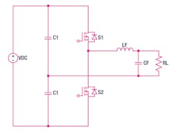
Figure 5 shows another use case with a half-bridge inverter topology. SiC MOSFETs are also widely adopted in UPS and renewable-energy applications as a replacement for silicon transistors. Again, the main advantages are higher attainable efficiency, improved power density, and higher operating temperature.
In particular, SiC MOSFETs can switch at higher frequencies, making it possible to use smaller-size passive components for more compact products and reduced solution costs. This is a big advantage for inverter applications where an LC or LCL filter is used on the output stage to filter the harmonics of the voltage generated by the switching stage. The size and cost of this filter can be significant if it must filter a low switching frequency.
The topology uses two SiC MOSFETs and two capacitors that split the dc bus voltage (Fig. 5, again). The output LC filter is connected between the midpoint of the bus capacitors and the midpoint of the switching leg. The two switches are typically controlled with sinusoidal pulse-width modulation (SPWM). The switching frequency is kept below 150 kHz to avoid high switching losses, although SiC MOSFETs have fast switching capability. Soft-switching techniques can reduce switching loss, although at the expense of additional components, increasing the cost and size of the converter.
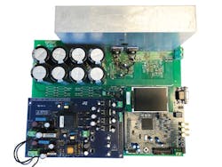
An example of such an implementation is shown in Figure 6 with a 2-kW half-bridge inverter topology operating from a 400-V dc bus and producing a 120-V ac rms output voltage. The SiC MOSFETs are two STGW90N65G2Vs in a HiP247 package driven by a high-voltage half-bridge gate driver capable of delivering up to 4 A of source/sink current. The selected gate driver, the L6491D, provides a driving voltage of +18 V/0 V to the gate of the two SiC FETs. The filter consists of a 250-µH inductor and a 470-nF plastic film capacitor.
We tested the inverter at 35, 70, and 140 kHz and summarize the efficiency results in Table 3, including the losses in the output filtering stage as well as power-supply and cable losses. The SiC MOSFET losses were calculated under the assumption that the inverter is operating at 2 kW and with a load having a power factor of 0.85.
In Table 4, the breakdown of the losses in the MOSFET is summarized for the three different switching frequencies. Observe that the 70-kHz switching frequency represents the best compromise in terms of losses and potential reduction of the size of the magnetic components.
Another interesting thing to note is the possibility of further optimizing the efficiency by using positive and negative gate-drive voltages of +20 V/−4 V. In this case, the efficiency results show an average improvement of 0.2% between 15% and 100% of the output load.
Figure 7 shows the case temperature for the two different driving schemes considered in this use-case example; the inverter is operating at room temperature with the nominal load (PF = 0.85) and a switching frequency of 70 kHz. The two SiC devices are mounted on a heatsink having a thermal resistance of 1.6C/W with natural convection.
Conclusion
In many areas of power conversion, traditional ac-dc converter topologies pose several limitations in all cases where high efficiency is a key requirement. This article illustrates how the properties of silicon carbide influence the performance of SiC transistors as well as the main relevant differences with Si-based IGBT switches.
Finally, we show two practical examples of a SiC transistor achieving very high efficiency.
