Mitigating EMI in Switch-Mode Power Supplies
Members can download this article in PDF format.
Switch-mode power supplies (SMPS) are the dominant type of power supply in electronic equipment today. Their small size and high efficiency make them desirable in virtually every kind of portable and battery-operated device, as well as ac-main-powered equipment. However, their use comes with tradeoffs, namely electromagnetic interference (EMI).
When packaged together with an SMPS, sensitive circuitry can be overwhelmed with EMI and fail to operate properly. As a power-supply designer, you’re responsible for determining what effect EMI may have on the operation of your product as well as other equipment in the same environment. Then you must initiate a design that will minimize the EMI while maintaining high efficiency with the power supply. Here, we’ll discuss this challenging design problem and present a mix of solutions to help you achieve that goal.
Sponsored Resources:
- Designing a low EMI power supply
- Optimizing pinout and pin placement to mitigate EMI in your power supply design
- Time-saving and cost-effective innovations for EMI reduction
Defining EMI
Electromagnetic interference involves broadband signals that can interfere with nearby circuits. EMI is particularly harmful to radio communications equipment, but it also impacts other circuits requiring high amplification.
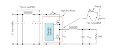
EMI is produced by switching circuits. The power MOSFETs in dc-dc converters are the main source of EMI, whose high-frequency, high-current pulses with their fast rise and fall times (dV/dt), ringing, and other discontinuities generate a wide spectrum of interfering signals.
EMI reaches the surrounding circuits via conduction or radiation. Conducted EMI travels by way of any common power and ground connections or even by parasitic inductances or capacitances. Radiated EMI is a radio signal that penetrates surrounding circuits. Both sources must be considered when designing solutions are considered. Conducted EMI is usually associated with low frequencies, typically less than 30 MHz. Radiated EMI is high frequency in nature and can extend from several hundred megahertz into the gigahertz range.
To determine the degree of EMI that a device can accommodate, some form of measurement or standard must be set. These measurements and standards are defined by regulatory agencies like the Federal Communications Commission (FCC) in the U.S. and the Comite International Special des Pertubations Radioelectriques (CISPR) in Europe. The FCC guidelines are defined in the Code of Federal Regulations (CFR) Part 15 subpart B. The CISPR guidelines are covered in CISPR 25 for the automotive industry and CISPR 32 for any multimedia equipment.
Adhering to these standards makes it possible to achieve electromagnetic compatibility (EMC). EMC means that the offending or generating equipment produces a level of EMI that will not negatively impact the equipment and application while the victim equipment is sufficiently protected. Thus, it will operate properly in the EMI environment. It’s essential that you become familiar with these standards and the testing methods used to certify and approve equipment for sale.
Standard Methods in Dealing with EMI
One trend that’s intensified the EMI problem is the increase in switching speeds in SMPS. Early supplies operated below 100 kHz. But, over the years, the quest for greater efficiency and smaller sizes has led to SMPS switching rates now exceeding many megahertz. These higher frequencies boost efficiency and help shrink filtering capacitors and inductors, significantly reducing power-supply size and cost. In turn, though, the EMI problem becomes even greater. However, some common and effective solutions have emerged.
The most obvious way to reduce conducted EMI is to use a brute-force filter at the input to the switch-mode regulator (see figure). Rectified dc is applied to large capacitors that will remove much of the EMI, but usually smaller capacitors and series inductors, and occasionally ferrite beads, are needed as well. This may be sufficient for some applications—it will only be evident through CISPR or FCC testing.
Another solution is to use what’s called spread spectrum or dithering the clock. This is the process of modulating the SMPS clock frequency. A low frequency (e.g., 9 to10 kHz) in the range of the resolution bandwidth (RBW) of the measuring instrument, as specified by the standard testing procedures, is used to vary the clock frequency over a range of ±5% to ±10%. This is generally more effective at the low EMI frequencies. The EMI signal fundamentals and harmonics are reduced, but it increases the noise floor.
Such a technique is implemented in some ready-to-use commercial regulator ICs if needed. A newer solution is to implement a digital spread-spectrum technique using two modulating signals to cover a wider range of frequencies.
Additional reductions in EMI can be achieved by employing an active filter facilitated by some IC regulators. The EMI is sensed, and an inverted polarity signal is generated to help cancel a significant portion of it.
Since a high percentage of the EMI is generated by the fast rise and fall times, reducing the slew rate is a good way to reduce emissions while maintaining an acceptable efficiency decrease. A common way of doing that is to insert series resistance in the drive path to the gates of the power MOSFETs.
All the methods previously discussed are used primarily to minimize low-frequency EMI (<30 MHz). Different techniques are needed to mitigate the EMI above 30 MHz. Some of these methods focus on the packaging of the regulator IC and in the PCB layout.
Additional EMI Reduction Methods
A major factor in reducing EMI is to minimize the high current loop area of the PCB layout. This current loop identified in the figure encompasses the high dV/dt nodes in the circuit. The golden rule in working with any high frequencies applies here: Keep all component leads and PCB traces short. This often-overlooked factor is one of the primary contributors to EMI. An optimized pin arrangement on the regulator IC makes external component placement simple and highly effective in minimizing loop size and EMI.
Texas Instruments offers its regulator ICs in a HotRod package that eliminates the standard bond wires from chip to package pin. The inductance of these short wires causes ringing in the power loop. The HotRod technique flips the chip and attaches it directly to the lead frame. This arrangement also reduces EMI by facilitating more effective connections to dc-dc converter input capacitors.
In extreme cases, further reduction in EMI can be achieved by shielding the power supply with an appropriate metallic enclosure or by using multilayer PCBs.
EMI mitigation is unique to each product, with many factors to consider. To learn more about these design methods and to investigate a product line of regulator ICs that make the process of reducing EMI simpler, faster, and more effective, look at these links. A comprehensive series of training videos is available to bring you up to speed quickly on EMI and its reduction.
Sponsored Resources:

