This Week in PowerBites: Advanced SiC Makes Design Quick
This article is part of the Power Management Series: This Week in PowerBites
SiC without Tears: Two Great Approaches to Simplifying the Design of SiC-Based Apps
Until recently, designers who wanted to take advantage of SiC's breathtaking power densities, switching speeds, and operating temperatures also had to deal with its finicky depletion-mode drive requirements, idiosyncratic switching behavior, and higher levels of EMI created by their sharp rise and fall times.
In response, several companies, such as UnitedSiC (covered in this blog), have developed a custom driver that’s co-packaged with the SiC FET feeding it with the inputs it needs to operate, and presents MOSFET-like characteristics to the outside world. The other class of solutions, such as Microchip Technology's dual-channel digital gate driver (also covered in this blog), uses an external chip to perform the same functions and carries with it a different set of advantages and tradeoffs.
Since both companies were making very significant product announcements that supported their approach to SiC on the same day, PowerBites has done its own version of "co-packaging" by presenting them together in this issue. Please feel free to compare, contrast, and share your insights with your fellow readers by writing me at bearberg (at) gmail (d0t) com.
Advanced 750-V SiC FETs Offer RDS(on) Values as Low as 6 mΩ
UnitedSiC's new family of advanced 750-V SiC FETs has moved wide-bandgap semiconductors another step toward becoming the Apex Predator in many high-power markets. Intended to address power designers' growing need for more efficient, more rugged, and higher-performing power devices, the family's highest-powered device offers 6-mΩ on-resistance, less than half of the nearest SiC MOSFET competitor, and a short-circuit withstand time rating of 5 ms.
The 6-mΩ device is one of nine new device/package options in the 750-V SiC FET series, rated at 6, 9, 11, 23, 33, and 44 mΩ, that deliver the high switching speeds and low losses needed for emerging applications. These include traction drives and on- and off-board chargers in electric vehicles and all stages of uni- and bi-directional power conversion in renewable energy inverters, power factor correction, telecoms converters, and ac-dc or dc-dc power conversion.
All of the new devices are based on United SiC's Gen 4 SiC FET “cascode” structure, which co-packages a SiC JFET power transistor with a silicon MOSFET gate driver that gives the device drive characteristics much like those of a conventional silicon device. Together, they provide the high speed, low losses, and high temperature operation of a SiC device. And they retain the stable, robust, and well-understood gate-drive characteristics associated with silicon MOSFETs, along with integral ESD protection.
For hard switching applications, the integral body diode of SiC FETs offers better recovery speed and forward voltage drop than competing Si MOSFET or SiC MOSFET technologies. Gen-4 devices also achieve reduced thermal resistance from die to case, thanks to advanced wafer-thinning techniques and use of a silver-sinter die-attach process.
During an interview with Electronic Design, Chris Dries, President and CEO of UnitedSiC, explained that the advantages of their new devices can be best understood when quantified by figures of merit (FOM) such as RDS(on) × A, a measure of conduction losses per unit die area.
"FOM RDS(on) × EOSS/QOSS is important in hard-switching applications, while FOM RDS(on) x COSS(tr) is critical in soft-switching applications," said Dries. "And I'm pleased to say that our Gen-4 SiC FETs achieve the lowest values in the market at both high and low die temperatures. Their FOM RDS(on) x EOSS/QOSS is half the nearest competitor values, while their FOM RDS(on) x COSS(tr) device values are around 30% less than competitor parts—and those devices are rated at 650 V compared with UnitedSiC’s at 750 V."
All of the devices are available in the TO-247-4L package, while the 18-, 23-, 33-, 44-, and 60-mΩ devices also come in a TO-247-3L package. Pricing (1,000-up, FOB USA) for the new 750-V SiC FETs range from $4.15 for the UJ4C075044K3S, to $23.46 for the UJ4SC075006K4S. All devices are available from authorized distributors.
Visit www.unitedsic.com for more information.
Configurable Digital SiC MOSFET Gate Driver Cuts Switch Losses Up to 50%
Microchip’s AgileSwitch 2ASC-12A2HP 1200V dual-channel digital gate driver represents a well-executed example of the other popular approach to taming the unruly characteristics of silicon-carbide power devices we discussed at the top of the blog.
Since Microchip already has a broad portfolio of discrete SiC MOSFETs and SiC power modules, it's no surprise that the company announced a new production-ready, 1200-V dual-channel digital gate driver. In addition to allowing you to drive a SiC power device using signal levels typically meant for silicon MOSFETS, Microchip’s AgileSwitch 2ASC-12A2HP is configurable. Thus, it can be optimized to influence dynamic issues with some of the less savory aspects of SiC devices, such as voltage overshoot, switching losses and electromagnetic interference.
The switch has been targeted (and qualified) to for use in EVs, chargers, locomotives, and higher-powered industrial/military vehicles. However, its versatility should also help SiC find its way into lots of equipment that supports renewable energy and micro-grid systems.
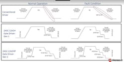
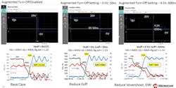
The AgileSwitch's configurable feature set includes a heavily-upgraded version of its pervious Augmented Switching functionality that shapes the rising and falling edges of the drive pulse to minimize switching losses, reduce EMI, and provide better protection in the event of a fault condition. While the earlier version could only massage the trailing edge of the drive waveform, the new version can be configured to adjust the slopes of both the turn-on and turn-off waveforms, and add step functions for turn-on (two steps), turn-off (three steps), and short circuit protection (four steps).
Together, they can dampen drain-source voltage (Vds) overshoots by up to 80% and slash switching losses by as much as 50%. The gate driver is able to source/sink up to 10 A of peak current and includes an isolated dc-dc converter with low capacitance isolation barrier for pulse-width-modulation (PWM) signals and fault feedback.
Other features include:
- 28-V maximum output driver voltage (VCCA-VSS)
- Fast response time DSAT protection
- Supply undervoltage (UVLO) protection
- Supply overvoltage (OVLO) protection
- Temp sense/protection with NTC, PTC, or RTD
- High-voltage dc link monitoring/protection
- Gate Miller clamp option
- Digital configurable blanking time
- Digital configurable deglitch for trigger and DSAT input
Applications
In addition to commercial vehicles, Microchip says the gate driver's automotive temperature rating and other qualifications make it well-suited for other applications such as charging infrastructure, energy-storage systems, solar inverters, and aircraft flight actuators.
Development Tools
The 2ASC-12A2HP gate driver can be evaluated, optimized, and configured using the latest release of Microchip's Intelligent Configuration Tool (ICT) software platform. This interface allows users to configure gate-driver parameters including the gate switching profiles, system critical monitors, and controller interface settings. The ICT has starter settings for many commercially-available SiC switches and works with a family of module adapter boards to help designers connect to several different footprints, as well as the company’s Augmented Switching Accelerated Development Kits (ASDAK). The result is a gate driver that’s tailored to their applications without having to change hardware.
Availability
The AgileSwitch 2ASC-12A2HP digital gate driver is available now for volume production; visit the purchasing portal or contact a Microchip authorized distributor. For additional information, contact a Microchip sales representative, authorized worldwide distributor, or visit Microchip’s website.
Next-Gen Supercaps Provide Backup Power for Critical Automotive Electronics
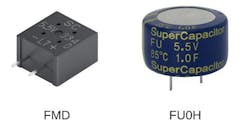
The FMD and FU0H series of high-performance supercapacitors developed by KEMET are intended for critical automotive electronic systems that require a main power system backup during a power loss, such as ADAS, autonomous vehicles, and central gateway ECUs. Their high capacity, long lifetime, and wide temperature range also makes them a good backup-power option in IoT devices, smart meters, medical devices, and industrial computing.
Members of both families deliver 1,000 hours at 85°C/85% RH-rated voltage and operational temperature ranging from −40 to 85°C. The FMD series offers the highest lifetime with up to 4,000 hours. These supercapacitors are manufactured in an ISO TS 16949 certified plant, qualified to an automotive testing protocol, and are subjected to PPAP/PSW and change control. Depending on the type of load and current demand, they can store enough energy to provide backup for durations ranging from a few seconds to several hours.
KEMET’s miniature supercapacitors use a proprietary aqueous electrolyte solution that provides high durability against liquid leakage, vibrations, and thermal shock found in automotive and industrial applications. As a result, the service life of these supercapacitors exceeds the vehicle's lifetime, eliminating service issues related to finite lifetimes of Li-ion cells. The supercapacitor’s benign open-circuit failure mode contrasts with typical short-circuit battery failures that may result in outgassing or ignition.
To learn more about their capabilities and applications, visit https://www.kemet.com/en/us/new-products.html.
Smart BLDC Drivers with Configurable Firmware Target Motors Up to 70 W
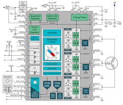
Texas Instruments unveiled a series of brushless dc (BLDC) motor drivers that support sensorless operation and enable code-free development of industrial and medical products, including major and small home appliances, ventilators, and continuous positive airway pressure (CPAP) machines.
Capable of driving motors requiring up to 70 W, using either trapezoidal or field-oriented control (FOC) drive algorithms, the drivers integrate a powerful embedded real-time controller, power MOSFETs, and several other discrete devices in a single package that uses up to 70% less board space. The devices feature configurable on-chip code that enables developers to spin a BLDC motor in less than 10 minutes after unboxing the development system, and then quickly optimize its parameters to their application's requirements.
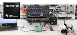
The MCT8316A, a sensorless trapezoidal control motor driver, can support switching speeds of up to of 3.5 kHz. It allows designers to tune a motor using only five hardware pins, simplifying systems by eliminating the need for a microcontroller interface. The MCF8316A is a sensorless FOC motor driver that can automatically extract the critical electrical parameters from its target motor, enabling it to deliver consistent system performance regardless of manufacturing variations.
Both devices integrate three gate drivers and six high- and low-side MOSFETs with 50 mΩ of on-state resistance (RDS(on)) each. They’re the first BLDC motor drivers to enable up to 70 W of power with 8 A of peak current for 12- and 24-V systems. In addition, they integrate components such as a low-dropout regulator, dc-dc step-down regulator, and current-sense amplifiers, eliminating as many as 18 discrete integrated circuits.
Software Acoustic Control
Both drivers' firmware also supports fault detection/protection functions and can be tuned to reduce the motor's acoustic emissions for quiet, efficient operation in applications such as air purifiers, refrigerators, washing machines, and fans. The MCF8316A features a patented, precise automatic dead-time compensation technique that compensates for current distortion, allowing engineers to optimize motor acoustic performance. It also includes variable trapezoidal control techniques that designers can use to reduce motor noise.
Additional information on acoustic emission reduction techniques can be found in the application brief, “How to Reduce Motor Noise with Code-Free, Sensorless BLDC Motor Drivers.”
Packaging, Availability, and Pricing
Pre-production versions of the MCF8316A and MCT8316A are available exclusively on TI.com in a 40-pin, 5- × 7-mm quad flat no-lead package. Pricing starts at US$1.75 in 1,000-unit quantities. For more information, see www.ti.com/mcf8316a-pr and www.ti.com/mct8316a-pr.
For additional details on their impact on the development cycle, read “3 ways to speed cycle time when designing with brushless-DC motors.”
Push-Pull Transformers Boost Isolated Power Performance for Serial Communications
Bourns' Model PAD00x-T764 Isolation Transformer Series features functional isolation and a low 0.4-mm-profile form factor to simplify isolated power and serial communication signal integrity. Designed to support CAN, RS-485, RS-422, RS-232, SPI, I2C, and lower-power LAN-based applications, the transformers are well-suited for industrial automation, embedded solutions, ac motor drives, system integration, communication PHYs, smart metering, and many other applications requiring low dc power.
Compatible with Texas Instruments’ SN6501 and SN6506B, Maxim’s MAX253 and MAX845, Analog Devices’ ADM2485, and similar transformer drivers, Bourns’ Model PAD00x-T764 series 3.1 kV ac withstanding voltage rating provides a strong isolation barrier from high-voltage hazards, such as high-voltage batteries. Their ferrite toroid core helps ensure a high coupling factor and heightened efficiency.
The series offers 3.3- to 5-V input, standard 3.3- to 10-V output, and up to 250-mA output with various turns ratios. The Bourns Magnetics product line also supports most modification and customization requests for this push-pull transformer series.
The Model PAD00x-T764 Series isolation transformers, available now, are RoHS compliant and halogen free. For more detailed product information, visit www.bourns.com/products/magnetic-products/transformers-power.
High-Power Wireless-Charging Chipsets Deliver Up to 70 W with High Efficiency
STMicroelectronics’ STWLC98 integrated wireless power receiver can provide mobile and portable devices with faster wireless charging and flexible charge-sharing capabilities. When combined with the STWBC2-HP transmitter IC, the complete transmitter-receiver system offers up to 70 W on the receiver end at high system efficiency.
The STWLC98 can fully charge today’s premium smartphones, which contain high-capacity batteries, in just under 30 minutes. Compliant with the Qi EPP 1.3 wireless-charging standard commonly used in the smartphone industry, the STWLC98 is managed by a 32-bit Arm Cortex-M3 core that supports a range of features including built-in protection. It comes with an embedded OS that simplifies Qi 1.3 standalone certification.
On the transmitter side, the STWBC2-HP can work with ST’s STSAFE-A110 secure element to store official Qi Certificates and provides authentication that leverages state-of-the-art cryptography. Support for the Company’s innovative ST Super Charge (STSC) protocol enables fast charging up to the maximum power-transfer rate of 70 W.
Free to Move About the Cabin
The STWLC98 features ST’s proprietary Adaptive Rectifier Configuration (ARC) mode that enhances the ping-up and power-transfer spatial freedom of the system in both horizontal and vertical directions without any change in hardware or coil optimization. Enabling ARC mode, which transforms the whole surface of the transmitter as usable charging area, increases the ping-up distance by up to 50% in all directions.
The STWLC98 works directly with the STWBC2-HP, which contains a USB-PD interface; digital buck/boost dc-dc converter; full-bridge inverter; three half-bridge drivers; and voltage, current, and phase sensors. Controlled by a Cortex-M0+ core, the STWBC2-HP executes a patented fast PID loop and supports the STSC protocol.
With built-in power management, the STWLC98 has an energy-saving ultra-low-power standby mode. Total end-to-end charging system efficiency can exceed 90%, thereby complying with stringent eco-design targets. The power-charger chip features dedicated hardware and advanced algorithms that were developed to address challenges in ASK and FSK communication during high power delivery. Safety features include foreign object detection (FOD), which leverages high-accuracy current-sense IP; Q-factor detection; and robust communication between transmitter and receiver.
The STWLC98 also can operate in high-efficiency transmitter mode to allow for high-power charge sharing between devices. This is coupled with the STWLC98’s industry-first embedded Q-factor detection in a receiver device to ensure safe operation in transmitter mode.
Applications Abound
ST’s new 70W wireless-charging chipset creates a scalable solution that can be deployed in devices such as smartphones, tablets, laptops, power banks, True Wireless Stereo (TWS) devices, Bluetooth speakers, and AR/VR headsets. In addition, designers are able to extend fast and convenient wireless charging to medical equipment like monitors and medicine pumps, as well as cordless power tools, mobile robots, drones, and e-bikes. The chipset also is suited to automotive applications including in-cabin charging solutions and wireless charging of various modules on-board the vehicle.
Users of ST’s wireless power solutions can download and benefit from the free PC-based graphical tool, ST Wireless Power Studio, to accelerate design-in and simplify processes including calibrating FOD, tuning Q-factor detection, and communication diagnostics.
Pricing and Availability
Both devices are in high-volume mass production. The STWLC98 is packaged as a 4.3- × 3.9-mm, 90-bump, 0.4-mm-pitch WLCSP, priced from $2.60. The STWBC2-HP comes in a 8- × 8-mm, 68-pin, 0.4-mm-pitch VFQFPN, with pricing from $3.30. For further information, go to www.st.com/wireless-charger.
Read more from the Power Management Series: This Week in PowerBites
