How to Miniaturize Your Power Supply
This article is part of the TechXchange: Power Supply Design
Members can download this article in PDF format.
Miniaturization has always been a pervasive theme in the electronics industry and is especially important for power supplies. The quality of a power supply is often expressed in terms of power per volume. This article discusses a few power-supply design considerations that can help achieve miniaturization.
Minimize the Number of External Components
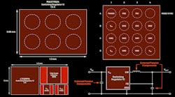
A power supply normally consists of at least one semiconductor and passive external components such as an inductor, capacitors, and a few resistors. Reducing the number of components to those shown in Figure 1 is the first step toward shrinking the size of the overall power supply.
If other functions, such as an adjustable output voltage or an adjustable soft-start time, are needed, it increases the number of passive components and thus the space requirements for the overall solution. The circuit in Figure 1 is an example of a switch-mode buck converter with a minimal number of required passive components.
Minimize the Size of External Components
For the smallest possible output capacitor and inductor sizes, the switching-regulator IC must have the highest possible switching frequency. The voltage ripple of the output voltage primarily behaves linearly with respect to the value and thus the size of the external components. For example, if the switching frequency is doubled, the required inductance value is halved for the same output voltage ripple. This allows for smaller designs.
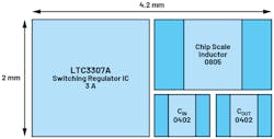
Figure 2 shows the space requirements of an LTC3307A switching regulator. Due to the high switching frequency of 3 MHz, a small inductor can be used.
Minimize the Size of Switching-Regulator IC
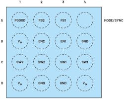
The LTC33xx platform from Analog Devices consists of switch-mode step-down voltage converters that convert with high switching frequencies of up to 5 MHz. For example, the LTC3315A has been optimized for space-constrained applications. It’s a dual converter with two channels that can each deliver 2 A of output current in a 1.64- × 1.64-mm wafer-level chip scale package (WLCSP) (Fig. 3).
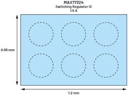
Another example is the MAX77324 single-channel step-down switching regulator. It has an output current maximum of 1.5 A and comes in a 1.22- × 0.85-mm housing. Figure 4 shows the MAX77324 package footprint.
Reduction in Size Through Integrated Inductor
A different way to reduce the power-supply circuit size is to combine the inductor with the switching-regulator IC. This combination is called a module. Integration makes it possible to reduce the edge length by allowing the inductor to be placed on the semiconductor IC.
Another miniaturization obstacle also can be overcome by using the inductor in the module as a thermal conductor and a heatsink. With the proper connection of the inductor to the silicon within the power module, heat from the semiconductor can be dissipated extremely well. Especially for small switching-regulator ICs with high output currents, heat dissipation is becoming a bigger problem because the silicon can’t be used above the maximum allowable operating temperature.
There are many ways to reduce the size of a power supply using innovative techniques. This brief power-management tip covered a few of them. Miniaturization brings with it additional, indirect advantages, such as lower costs due to smaller board space requirements, the possibility of building technical devices with higher functionality and thus greater benefit, and even lower transport costs due to smaller and lighter electronic devices.
Read more articles in the TechXchange: Power Supply Design


