Making Zero the Hero in AC-DC Conversion
What you’ll learn:
- ZVS and its benefits.
- New power-conversion architectures that optimize efficient power conversion by supporting ZVS soft switching.
In recent years, the discussion has grown about zero voltage switching (ZVS) as the ideal route to increase the efficiency of ever-higher-frequency ac-dc power-conversion designs without impacting EMI performance. However, achieving such “soft” switching is difficult, especially across the varying range of loads and input and output voltages that are now common in applications such as universal USB chargers.
Many conventional LLC converters, for example, use resonant ZVS to achieve high efficiencies at high and full loads for a given input voltage. Unfortunately, they suffer as the load reduces or the input voltage changes, and hard switching losses start to become more prevalent.
This article explores ZVS and its benefits and look at the challenges of delivering ZVS in conventional ac-dc conversion applications. It also introduces techniques that “flatten” the efficiency curve by enabling ZVS soft switching across a much wider load range and input and output voltage ranges, with practical examples.
The Need for High Efficiency
Efficiency is one of the most important aspects of power conversion, as so many benefits flow from a highly efficient design. By ensuring that as much of the input power is delivered to the output as usable power, heat generation within the power converter is minimized.
First, this reduces operating costs, especially at high power levels. It also means that with less heat to remove, the design can be smaller, often requiring few (if any) thermal design measures. This makes the solution simpler, lighter, and lower cost—three of the key challenges often faced by designers.
In the past, efficiency was usually quoted at a single load point and, of course, this was where the efficiency was best. However, systems (especially those with dynamic loads) rarely operated at these “optimum” points and, consequently, the actual efficiency seen was often far lower than the “headline”’ figure, especially at low loads.
To address this, efficiency requirements evolved to stipulate minimum efficiency levels at multiple load levels. Perhaps the best known is the “80 PLUS” standard that defines required efficiencies at 20%, 50%, and 100% load, with its most basic level requiring at least 80% efficiency—even at 20% load. The highest level (“Titanium”) mandates 90% efficiency at 10% load.
As a result of this voluntary standard, there’s a far greater awareness of efficiency at both lower load levels and during standby. Achieving requisite efficiency requires advanced or innovative topologies and high-end semiconductors, including wide-bandgap (WBG) devices based on silicon carbide (SiC) and gallium nitride (GaN).
Zero Voltage Switching
MOSFETs exhibit two types of loss: static and dynamic. The static loss is due to the resistance between drain and source (RDS(ON)), while the dynamic losses, which occur every switching cycle during the turn-on and turn-off of the device, increase in proportion to frequency. Designers are seeking to increase the frequency of operation to reduce the size and weight of magnetic components. As a result, these dynamic losses must be addressed.
Hard switching has a number of downsides, including the energy dissipation, the stress put on the MOSFET, and the EMI generated, which is proportional to the voltage across the MOSFET (VDS) and the switching frequency.
Quasi-resonant (QR) flyback converters go some way to minimizing the losses and reducing EMI by ensuring that the turn-on occurs when VDS is at a minimum—or in a “valley”—hence the name “valley switching.” At full load and with U.S. input voltage, the QR flyback has excellent performance, as it’s almost ZVS. However, in other working conditions, the valley is too far from zero, and it incurs hard-switching losses.
Soft-switching (or ZVS) techniques are able to ensure that switching only occurs when VDS = 0. In this approach, the MOSFET turn-on transition losses (which are the most critical losses) are zero, irrespective of the operating frequency and input voltage.
Soft switching significantly improves efficiency and brings other benefits such as elimination of COSS discharge losses and high peak currents. The gate drive also is somewhat simplified as there are no “Miller” effects. Another possible enhancement is the addition of an regenerative clamp that can be used to recover energy from leakage inductance, while also suppressing voltage spikes on the main MOSFET.
With the huge breadth of power requirements, it’s important that the solution is tailored to the application. Relatively small differences in requirements can lead to significant differences in results. For example, for a small power adapter QR is a valid choice, because it’s able to operate close to zero volts and losses are small.
However, that does depend on the input voltage. For example, in the U.S. and Japan, mains voltages are lower, and this solution works. However, in the European Union (and U.K.), at low load a QR circuit is unable to discharge the parasitic FET, causing hard switching losses.
Active clamp flyback is often used to resolve this issue, but it’s an expensive solution due to the high-side high-voltage FET that’s required to carry high current. Despite the cost, it’s a reasonable solution above 50% load. Below this, though, it operates in burst mode, which degrades the efficiency.
New Ways to Implement ZVS
One example of the latest methods that’s being used to address ZVS is the EcoVoltas family developed by Eggtronic. It maximizes efficiency across the load range while minimising standby power consumption, facilitating the ability to meet modern efficiency requirements.
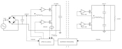
To address higher-power applications that require front-end power factor correction (PFC), Eggtronic’s SmartEgg (Fig. 1) is a single-stage PFC + ac-dc converter that acts simultaneously as a PFC and isolated regulator. A traditional approach requires three stages (boost PFC, dc-dc buck, and resonant LLC), so the removal of one stage immediately provides efficiency gains. SmartEgg is suited to applications in the 100-W to 1-kW range, including high performance laptops, TV panels, and home appliances.
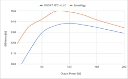
Based on the company’s EPIC101AGSE01 32-bit mixed-signal controller, SmartEgg offers optimized low-power and no-load performance. It features an integrated ZVS gate driver and customizable support for power delivery (PD) as well as protection against overvoltage, brownout, overpower, overcurrent, and overtemperature. According to the company, efficiency performance compared to a boost PFC + LLC solution increases significantly (Fig. 2), most notably at lower power levels, achieving around 92% efficiency at 10% load.
In addition, SmartEgg reduces the component count compared to a boost PFC + LLC solution. The latter requires eight MOSFETs and two cores (RM7 and RM10), while the former needs only four MOSFETs and a single RM10 core. This simplifies the design as well as reduces the size and cost of the solution.
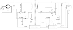
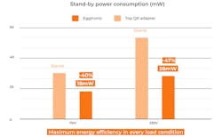
For lower-power (<100 W) applications such as USB-C power adapters, Eggtronic’s QuarEgg could come into play (Fig. 3). This high-performance flyback architecture is based on pulse-density modulation that uses forced ZVS at all load levels.In a QuarEgg solution, the EPIC101AFQE01 controller is located on the secondary side, allowing the usual optocoupler to be replaced with a lower-cost signal transformer. The EPIC controller is capable of multimode operation for flat efficiency, and it’s optimized for low power and no-load efficiency. It shows at least a 40% improvement in standby power consumption over legacy QR designs (Fig. 4).
Like the SmartEgg, it has an integrated ZVS gate driver, PD support, and a range of protection features. The QuarEgg EPIC controller also includes integrated cable drop compensation and frequency jittering that reduces the EMI signature of the solution.
Design Support
Reference designs are available for both solutions so that designers can become familiar with the technology and build their own designs. The 80- × 62- × 28.2-mm (17.6 W/in.3) SmartEgg board offers 150-W nominal power. No-load power consumption is 137 mW with 110-V mains input, and the power factor is >0.9.
The QuarEgg board, measuring 38.3 × 38.3 × 18.6 mm (21.02 W/in.3), is rated at 35 W nominal. No-load power consumption is under 18 mW with 110-V mains input. Both boards are capable of passing all global EMI requirements.
Summary
Energy efficiency in power conversion has always been important. However, with increasing environmental awareness, a desire for smaller solutions, and rising energy costs, its prominence is on the rise. As a result, design goals are becoming more challenging, requiring high levels of efficiency right across the load profile—as well as low levels of standby and idle consumption (which represent most of the energy losses for electric and electronic devices always connected to the grid).
Techniques such as ZVS and active clamp can enhance efficiency and manage EMI, but when implemented discretely, they can have significant BOMs and high costs, Moreover, they’re typically not able to optimize light load efficiency. To help mitigate those issues, solutions such as Eggtronic’s QuarEgg and SmartEgg can deliver higher levels of performance at lower cost points.
The EcoVoltas range continues to evolve in response to customer needs. Likely future versions of QuarEgg will include a primary-side controller version and a single-output solution with a significantly reduced BOM. SmartEgg will expand to include a fixed-voltage battery-charger solution as well as a 140-W PD solution and a USB 3.1 design.


