Creative Spins on Low-Iq Applications and Designs (Part 1)
This article is in TechXchange: Why Low Iq is the Smart Thing to Do.
Members can download this article in PDF format.
What you'll learn:
- Three key parameters when considering Iq in IC designs.
- Different and perhaps unique approaches to build low-Iq designs.
Many tech designers think about integrated-circuit (IC) quiescent current (Iq) as shutdown current, or standby current, or even no load current. All three terms are virtually the same, that is, the input current drawn by an IC from its input supply. The input current to an IC is impacted by various states in several ways.
When looking at an IC datasheet, the three most important parameters that designers must understand and consider in their designs are shutdown current, non-switching current, and no-load input current:
- Shutdown current is defined as the current being drawn when an IC is disabled, leading to a state of zero voltage at the IC output.
- Non-switching current is when an IC is enabled and in between switching events.
- Operating quiescent current is also known as standby current, no-load input current, ground current, operating Iq, switching Iq, no-load Iq, sleep mode, and more.
The above terms all refer to the state in which the device is enabled, and is regulating, with a zero load current on the output.
Among the unique, and yet pertinent, design applications for low Iq include:
A digitally assisted, dual-loop (DADL) LDO regulator
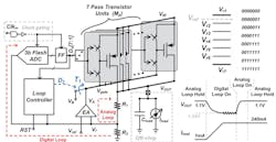
This kind of architecture combines two key kinds of regulators: analog and digital low-dropout (LDO) devices (Fig. 1). In this design, a dual-loop LDO uses its digital loop for coarse tuning and its analog loop for fine-tuning.1 The loop controller (LC) is designed by a finite state machine (FSM), which makes sure that no conflicts exist between the digital and analog loops.
The LDO design has achieved a 245-mA maximum load current. The power-supply rejection (PSR) was −42/−34 dB at 1 MHz for a 0.5-/240-mA load current and the maximum voltage droop was 71 mV with a recovery time of 520 ns for a load step of 240 mA. The figure of merit (FOM) was 7.4 ps.
An LDO with dynamic biasing super-buffer technique
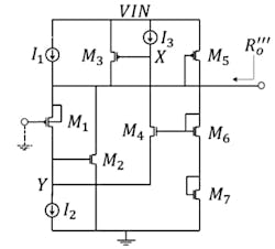
A standard super-buffer architecture isn’t able to adjust its Iq under no-load or light-load conditions due to the static biasing voltage (VB), which is at the M4 gate. To rectify this, designers added a dynamic biasing structure (M5, M6, and M7) to the M4 gate (Fig. 2).2
A buck-converter design with dead-time control and automatic power-down system for wireless sensor networks
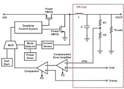
Physical or environmental conditions can be monitored via a wireless network designed with spatially distributed autonomous devices which use sensors. These types of networks are typically deployed in remote and difficult to access locations. In cases like this, energy harvesting is usually part of the design to charge the batteries in the wireless sensor network. Many of these systems deploy a power-scavenging technique to charge the power-supply batteries (Fig. 3).3
Designing a solid power-management system will prevent failure to transmit, record, and detect data, reducing the likelihood of frequent maintenance visits. Designing these systems with low-power regulators and creative methods to reduce system power consumption must be implemented. Switching buck converters are frequently used for such high-efficiency and low-power systems.
A 5-V dynamic class-C amplifier (DCCA) with paralleled single-stage and near-zero dead-zone (NDZ) control and current-redistributive rail-to-rail Gm-boosting technique
A very key analog block in a VLSI design is the buffer amplifier, which is dedicated to driving large, off-chip loads. Achieving a fast settling time and high output-current drivability that can range over a wide input voltage is quite challenging to designers if they want low-Iq consumption.
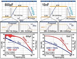
The top of Figure 4 shows the measured response with a step input of Δ4.2V.4 With a load capacitance (CL) of 800 pF, the proposed amplifier achieved rising and falling slew rates (SRs) of 10.3V/μs and 10.2V/μs. At CL = 10nF, rising and falling SRs of 0.83 V/μs and 0.86 V/μs, respectively, were obtained.
Also, due to the benefit of the DCCA with NDZ, averaged 1% settling times of 540 ns and 6.5 μs were measured at CL = 800 pF and 10 nF, respectively. The bottom of Figure 4 shows the measured frequency response. Gain bandwidth (GBW) and phase margin were measured to be 127 kHz (10.5 kHz) and 58.6 degrees (84 degrees), respectively, at CL = 800 pF (10 nF).
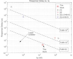
A 0.75- to 5-V, 15.8-nA with 1.8-μs delay supply voltage supervisor (SVS) using adaptively biased comparator and sample-and-hold technique for IoT
This design features a very-low-Iq, fast-response SVS that’s perfect for use in low-power, fast response power-management applications. Verified by experimental results from test chips, the design demonstrates a power-delay FOM of 29 (Fig. 5).
This article shows a fully autonomous, lowest-monitored SVS at 0.75 V at the date of posting in 2021.5
A 220-nA Iq capacitor-less LDO regulator with improved recovery time
This ultra-low-Iq, capacitor-less low-dropout regulator (CL-LDO) uses an improved single transistor control (STC) and adaptive structural transformation. It allows the regulator to have a fast recovery time at ultra-low-level quiescent bias currents.
CL-LDO regulators experience a traditional design tradeoff, whereby reducing current consumption to under 1 µA will compromise transient FOM. Also, when providing loop stability at all load currents, a main design issue will have to be addressed at the circuit level by employing different frequency compensation schemes. This tradeoff—employing an adaptive structural transformation from a single-stage LDO topology to a two- and three-stage cascaded topology—is examined in Reference 6.
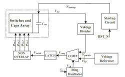
A switched-capacitor step-down converter with 34-nA Iq and a 1.2-V output at 0- to 5-µA load current
Implantable medical devices need ultra-low power, especially in a switched-capacitor dc-dc converter. This type of converter is controlled via a hysteretic (switching frequency that’s not fixed) control method, which uses a clocked comparator in place of the traditional error amplifier (Fig. 6).7
With this approach, no compromise is needed between the bandwidth and stability. The switching frequency may be calculated; however, it will depend on the power supply voltage, load voltage, and inductor values in the circuit.
1.88-nA-Iq CL-LDO regulator with adaptive biasing based on a super-source-follower absolute voltage difference meter
The CL- LDO regulator in this application has an adaptive biasing error amplifier (EA).8 This method ensures reduced quiescent power consumption and enables a high drive capability in dynamic operation. It uses a super source follower (SSF), which is an improved voltage follower that can deliver a maximum output current at the milliamp level—far higher than its quiescent bias current at 1.88 nA.
Part 2 of this series will present eight other low-Iq applications for designers.
Read more articles in TechXchange: Why Low Iq is the Smart Thing to Do.
References
1. “A 245-mA Digitally Assisted Dual-Loop Low-Dropout Regulator,” IEEE Journal of Solid-State Circuits, Vol. 55, No. 8, August 2020.
2. “A Power-Area-Efficient Low-Dropout Regulator with Enhanced Buffer Impedance Attenuation,” School of Electronics and Information Technology, IEEE 2019.
3. “Design of Buck Converter with Dead-time Control and Automatic Power-Down System for WSN Application,” 2019 IEEE Wireless Power Transfer Conference (WPTC).
4. “A 5V Dynamic Class-C Paralleled Single-Stage Amplifier with Near-Zero Dead-Zone Control and Current-Redistributive Rail-to-Rail Gm-Boosting Technique,” ISSCC 2021, Session 5, Analog Interfaces 5.8.
5. “A 0.75-5V, 15.8 nA with 1.8 μs Delay Supply Voltage Supervisor using Adaptively Biased Comparator and Sample & Hold Technique for IoT,” IEEE CICC 2021, Session 17: DC-DC Converters, Paper 17-7.
6. “A 220-nA Quiescent Current Capacitor-Less Low Dropout Regulator with Improved Recovery Time,” IEEE 2020.
7. “A 34 nA Quiescent Current Switched-Capacitor Step-down Converter with 1.2V output voltage and 0-5μA load current,” IEEE 2020.
8. “1.88 nA Quiescent Current Capacitor-Less LDO with Adaptive Biasing Based on a SSF Absolute Voltage Difference Meter,” IEEE 2020.

