Creative Spins on Low-Iq Applications and Designs (Part 2)
This article is in TechXchange: Why Low Iq is the Smart Thing to Do.
Members can download this article in PDF format.
What you'll learn:
- More different approaches to developing low-Iq designs.
- The role of LDOs in several design solutions.
Following on from Part 1, presented here are eight more unique, and pertinent design applications for low Iq.
A Low-Leakage-Retention LDO and Leakage-Based BGR with 120-nA Quiescent Current
This low-dropout (LDO) bandgap regulator (BGR) maintains very-low-leakage current consumption that lowers overall power consumption without the use of traditional bipolar junction transistors (BJTs).1 A 55-nm, 1-V CMOS process is employed in this design.
Ultra-low-power structures used in the design enable lower power-supply rejection ratio (PSRR) performance as compared to the other structures. This unique structure doesn’t apply any off-chip capacitor.
The design’s figure of merit (FOM) is defined as:
FOM = Tsettle × IQ/Iload = 1.7 ms x (120 nA/20mA) = 10.2 ns
An Adaptively Biased LDO Regulator with 11-nA Quiescent Current and 50-mA Available Load
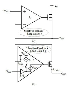
This design presents an LDO structure that regulates its output voltage with a series-series positive feedback loop that has an 11-nA quiescent current and a maximum available output current of around 50 mA (Fig. 1).2 Line and load regulations are quite competitive, and they were achieved through the proposed regulation scheme minus any load capacitor that’s usually needed for stability.
This LDO has current limiting and input reference current cancellation functions in its design architecture.
CMOS SRAM Test Based on Quiescent Supply Current in Write Operation
In this design, experiments were performed to examine if faulty CMOS SRAM integrated circuits (ICs) that are not able to produce the expected output. It can be flagged via measurement of the quiescent power-supply currents generated during write operations.3
This method is able to detect about 62% of faulty ICs using only a small number of test inputs, far better than conventional test methods. A test (March G) described in the referenced article detects all faults.
An Output-Capacitor-Free Synthesizable DLDO Using CMP-Triggered Oscillator and Droop Detector
This output-capacitor-free, synthesizable digital LDO (DLDO) is made up of fine and coarse loops.4 The system function here is able to sense a load voltage, which is in between reference voltages, that will activate the fine loop.
In the coarse loop, a comparator-triggered oscillator is used to create a high-frequency clock signal, without the probability of the comparator metastability, for fast regulation. Quiescent current ranges from 7.7 to 241 μA depending on the supply voltages.
Dual-Polarity Floating Battery for Class AB Output Stages with Accurate Quiescent-Current Control
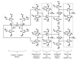
Previous structures were combined to create a floating battery exhibiting dual polarity and low-power dissipation for a Class AB output stage that’s able to use most any power supply.5 This circuit can operate at very low voltages that are close to transistor threshold voltages. It also can operate at quite high voltages while maintaining minimum power dissipation as well as accurate quiescent current control.
Unlike other approaches, the circuit doesn’t need an independent power supply, other than the one used to drive the Class AB output stage. The proposed circuit is shown in Figure 2.
Hybrid ET Supply Modulator IC with an Adaptive Quiescent-Current Controller for Its Linear Amplifier
This hybrid envelope-tracking (ET) supply modulator IC is based on a Class AB linear amplifier (LA) with supply voltage and temperature insensitive quiescent current (Iq) for dual-mode (ET/APT) operation.6
The referenced paper describes a further step for improving the efficiency of this circuit by modulating the supply voltage, for the LA in the ET supply modulator, corresponding to the average output power. An adaptive quiescent-current controller was able to modulate the LA supply voltage over a wider span of changing Iq temperature and voltage levels.
Quiescent-Current Control for Low-Distortion Linear Power Amplifier
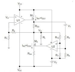
In this design, a quiescent-current control scheme was developed for a linear, Class A power amplifier that led to low amplification distortion with no zero-crossing distortion (Fig. 3).7
The amplifier push-pull output transistors were biased to be minimally on to avoid any disadvantageous effect from crossover distortion in addition to exciting the distortion when the output transistors turn on.
This circuit offers the freedom to separately adjust the quiescent currents in the push-pull output transistors. It also reduces the difficulty of the design, as well as being able to maximize the circuit headroom usage.
Simulation results confirm that this circuit architecture is able to raise the energy efficiency of a Class A amplifier to 74%, placing it very near the Class B amplifier’s 78.5% efficiency.
Zero-Quiescent-Current, Delay-Adjustable, Power-on-Reset Circuit
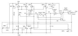
Power-on-reset (POR) circuitry is of utmost importance in mixed-signal as well as digital integrated circuits (ICs). POR circuitry initializes the critical nodes in the analog and digital circuits, inside of an IC, while the power supply is ramping up.
The unique circuitry concept of a POR circuit is demonstrated in this design,8 having a zero quiescent current in addition to an adjustable delay (Fig. 4).
This circuit was fabricated with a 0.5-µm technology and a wide power-supply span of 1.8 to 5.5 V. The circuit generates a POR signal that’s independent of the power-supply ramp time over a wide temperature range of −40 to +125°C.
Summary
In this article, we’ve demonstrated a variety of unique circuit designs that feature very low quiescent-current levels. Operating at such levels will directly result in high conversion efficiency at light loads.
Read more articles in TechXchange: Why Low Iq is the Smart Thing to Do.
References
1. “A Low Leakage Retention LDO and Leakage-based BGR with 120nA Quiescent Current,” IEEE 2021.
2. “An Adaptively Biased LDO Regulator with 11nA Quiescent Current and 50mA Available Load,” IEEE 2021.
3. “CMOS SRAM Test Based on Quiescent Supply Current in Write Operation,” IEEE 1995.
4. “An Output-Capacitor-Free Synthesizable Digital LDO (DLDO) Using CMP-Triggered Oscillator and Droop Detector,” IEEE 2007.
5. “Dual-Polarity Floating Battery for Class AB Output Stages with Accurate Quiescent Current Control,” IEEE 2007.
6. “Hybrid ET Supply Modulator IC with an Adaptive Quiescent Current Controller for Its Linear Amplifier,” 2021 IEEE/MTT-S International Microwave Symposium.
7. “Quiescent Current Control for Low Distortion Linear Power Amplifier,” IEEE 2015.
8. “Zero Quiescent Current, Delay Adjustable, Power-on-Reset Circuit,” Texas Instruments 2014.


