Reducing the Cost of Test With Boundary Scan
Despite its standardization as IEEE 1149.1 in 1990 and wide use in the industry, many test engineers and developers still do not fully understand the benefits of boundary scan test. The misconceptions regarding this well-established technology, also known as JTAG test, have led to its relatively slow acceptance or complete rejection by some companies. Here are some reasons why acceptance of boundary scan test has been slow:
- Cannot thoroughly test a UUT.
- Limited test applications.
- Limited number of components supporting the technology.
- Cost to purchase and use boundary scan components.
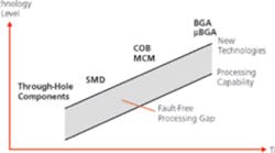
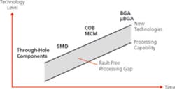
Figure 1. Development of New Technologies
Despite enormous manufacturing improvements, production problems and component failures do occur. New package types, higher pin-count devices, and denser layouts on PCBs continue to challenge the manufacturing process, as shown in Figure 1.
The installation of large, complex chips continues to be an area for recurring faults. However, faulty assemblies must not reach the end user. The goal is to catch any fault as soon as possible in the production cycle by establishing an effective manufacturing test strategy.
The production process of a PCB must be analyzed to gain optimal quality at minimal costs. The main issue is failure analysis, with failure classification that helps determine the cause of the problem. Several test techniques can be used to check PCBs for failures. As an example, Table 1 shows common test technologies, their fault coverage, and the fault distribution in a production line of a German OEM.
Pros and Cons of Specific Test TechniquesTable 1 indicates that functional test (FT), in-circuit test (ICT), and flying- probe test (FPT) attain high test coverage of 90.8%. On the other hand, automated optical inspection (AOI) detects all faults except electrically defective components and faults caused by nonvisible solder joints, especially under ball grid arrays (BGAs).
The cons of these test techniques are listed in the following:
FT
- Test-program creation very time-consuming lasting weeks to months; average cost approximately $15k.
- Very high costs in repair due to limited diagnostics; well-trained personnel required for troubleshooting and fault isolation; average troubleshooting time: 30 min; cost approximately $20 per fault.
- Test of all functions (coverage of all possible faults) practically impossible.
| Fault Type | Fault Distribution In Percent | Functional Test | In-Circuit Test | AOI | Flying-Probe Test |
| Component??Mechanical Defect | 9.2 | Yes | |||
| Component??Electrical Defect | 21.3 | Yes | Yes | Yes | |
| Press-Fit Fault | 0.6 | Yes | Yes | Yes | Yes |
| SMT Placement Fault | 28.5 | Yes | Yes | Yes | Yes |
| THT Placement Fault | 7.3 | Yes | Yes | Yes | Yes |
| THT Soldering Defect | 4.1 | Yes | Yes | Yes | Yes |
| SMT Reflow Soldering Defect | 27.2 | Yes | Yes | Partly (13.6) | Yes |
| SMT Wave Soldering Defect | 1.8 | Yes | Yes | Yes | Yes |
| Coverage in Percent | 100 | 90.8 | 90.8 | 65.1 |
90.8 |
|
Table 1. Test Technologies and Test Coverage (Statistic Average Values) |
ICT
- High costs in test preparation due to UUT-specific test fixture; average cost $10k to $15k, more for highly complex fixtures.
- Extra costs when the UUT??s PCB layout changes.
- Storage and maintenance of test adapters very expensive.
- Probe placement more complicated due to ever-denser layouts.
- Impossible to access high lead-count BGAs via nails; unproductive to include in the layout and then probe extra test pads because the advantage of very large-scale integration (VLSI), namely the space savings, would be eliminated.
AOI
- Only visible features verified; fault detection at hidden solder joints not possible.
- No electrical test.
FPT
- High test execution time due to sequential probing of test points.
- Maintenance costs for worn probe tips and moving parts.
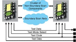
Boundary scan is possibly the most resourceful test technique, testing the connectivity on a PCB, similar to ICT, or between PCBs but without the need of physical contact to test pads (Figure 2). With only four lines, it drives and measures thousands of test points simultaneously, detects the failure location, and finds faults even under BGA components. While ICT requires specially constructed adapters, boundary scan testing is possible even if there is only one scanable component on the board.
Essentially, boundary scan means testing at the boundary of an IC. In addition to the core logic, special test logic is implemented in an IEEE 1149-compliant IC.1,2 Test points, or boundary scan cells, are put between core logic and physical device pins. To provide access to these test points, all boundary scan cells of a device are linked together to the boundary scan register, which is accessible from the outside through the test access port (TAP).
Figure 2. The Principle of Boundary Scan Test
Boundary scan test resources are very easily accessible, allowing them to be used throughout the entire product life cycle. Even before PCB layout is completed, boundary scan tests can be developed based on available schematic CAD data. No bed-of-nail fixture is needed so the layout information is not relevant for boundary scan test.
Test patterns created during the product design phase can be reused for prototype verification and debug as well as manufacturing test, repair, maintenance, and field service. This is an important advantage since, especially during the design of highly complex assemblies, testability throughout the product life cycle must be considered.
Due to elimination of the time-consuming adapter design, build, and verification process and the reusability of boundary scan tests, the time and effort required for testing and the cost of test itself are dramatically reduced. Only a few days or even hours are required to generate test programs compared with weeks or months for an ICT or FT. Boundary scan tests provide quick pin-level diagnosis while avoiding the high production, storage, and maintenance costs of bed-of-nail adapters.
In general, boundary scan detects the same faults as FT, ICT, or FPT (Table 2). Compared to other test techniques, boundary scan has a large financial advantage. In most cases, boundary scan leads to a significant cost reduction including considerably lower up-front investment and cost of ownership.
Where to Use Boundary ScanFigure 3. Example of PCB Type 1
For a better understanding of the following discussions, three different types of UUTs shall be considered:
Type 1—Single PCB, predominantly digital circuits; components with relatively small pin-count, no BGAs; and some components with boundary scan capabilities.
Type 2—Single PCB, predominantly digital circuits; components with high pin-count, a few BGAs; and some components with boundary scan capabilities.
Type 3—Single PCB, predominantly digital circuits; components with high pin-count, many BGAs; and most components with boundary scan capabilities.
Considering these three PCB types, boundary scan can achieve a reasonable reduction in the cost of test. The numbers provided in the following examples are average values; the savings can vary upward or downward for a specific UUT.
Type 1Type 1 is well suited for ICT. The cost-saving potential is in the combination of boundary scan with ICT, such as via boundary scan extension modules.
This PCB has approximately 1,200 component leads and 200 nets; statistically, the ratio of leads to nets is 6:1 (Figure 3). If there are three boundary scan-compliant components on the board with each connecting to 18 nets, then 54 nets or 27% of all nets are boundary scan accessible.
An adapter with 200 nails, each nail for one net, costs about $5,000. Of the total cost, 80% is proportional to the number of nails. By reducing the number of nails needed by 54, the savings achievable are 27% of $4,000 (80% of $5,000) or $1,080.
90.8
Table 2. Test Coverage of Boundary Scan (Statistic Average Values)
Type 2In this example, it is assumed that the manufacturer??s product variety is much wider. A flying probe is the most useful solution to test boards in such a low-volume, high-mix environment.
An average PCB shall have 560 nets and 3,200 components, with two boundary scan-compliant BGAs: one with 432 pins and the other with 256 pins. There are other high-pin-count components with 956 pins and an additional 230 low pin-count components on the PCB. A total of 5,114 FPT steps must be executed (device tests plus shorts tests on 10% of all nets). Assuming a rate of 13 test steps/s, the test time is 6.5 min.
The boundary scan resources in the BGA components offer potential savings. Testing these ICs via boundary scan can eliminate 1,376 FPT steps.
Statistically, the 688 BGA pins are connected to 115 nets (6:1 pin-to-net ratio) or 20% of all networks on this board. As a result, the number of nets to be tested for shorts, 56 or 10% of all nets, reduces by 20% to 45. The shorts test requires 1,035 steps (45 ?? 46 ?? 2), which results in 561 test steps less than the 1,596 steps necessary for 56 nets. The total reduction of test steps is 1,376 + 561 = 1,937 or 38% of all 5,114 steps, resulting in a cost saving of $2.74 per assembly.
In the case of a manufacturing capacity of 50,000 PCBs per year, the savings potential is $137,000, notably with just two boundary scan-compliant ICs on the UUT.
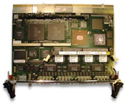
Type 3In this case, boundary scan testing is practically a no-brainer. The multitude of BGAs doesn??t allow any physical contacts so no other test technique really is efficient and useful (Figure 4).
The only alternative is X-ray inspection; however, the average investment required for an in-line system is about $300,000. Moreover, the test execution time on an X-ray system is greater by far than that of a boundary scan test.
A 430 mm ?? 380 mm PCB with 50 BGAs can be inspected by an X-ray system in 75 s (average value, test time of 700 ms per BGA plus total traversing time of about 40 s). In contrast, it takes approximately 10 s to test the entire assembly via boundary scan. The average cost for one test minute is calculated as $1. If the production volume were 50,000 PCBs per year, the reduction in test time would result in more than $50,000 in savings.
These are only three examples of how boundary scan can reduce the cost of test in electronics manufacturing. There are many other ways that it can be used to improve yield. For example, by combining boundary scan with AOI, the fault coverage can increase to nearly 100%. No other test technologies are required, and the quality of products shipped to the customer is very high.
For some applications, FT must be performed after structural testing to identify any dynamic failures that boundary scan and ICT or FPT could not catch. Again, a combination of boundary scan tools with functional test tools often times is very useful.
Last, but not least, the cost of repair and debug must not be ignored. In the production lines of the German OEM that provided the numbers used in this article, the costs amount to $7 per unit on average. However, if the fault is discovered by the end user, the cost increases dramatically to approximately $200. This means that a fault detected by the
Figure 4. Example of PCB Type 3
manufacturer before the product leaves the factory potentially saves $193 per faulty component.
If an assembly line produces 6,500 faults per year, a certain percentage of those faults most likely will not be discovered throughout manufacturing and final test. If there are appropriate test technologies or combinations, such as boundary scan with AOI in place to prevent just 5% of all 6,500 faults from slipping through the manufacturer??s tests, cost savings of more than $60,000 per year could be achieved.
SummaryThese examples demonstrate the enormous potential of boundary scan to decrease costs in the production process of PCBs. The same can be applied to system-level testing.
Boundary scan software has become faster and more user-friendly, and development in this direction will keep moving. New industries such as automotive electronics embrace boundary scan, and the number of combinations of boundary scan with various test technologies is increasing as well.
Today, you have a very wide range of test tools and a large number of components to select from, which makes implementing boundary scan easier than in the past, a trend that will last for many years to come. Ultimately, you can argue that not using boundary scan more often than not means losing valuable resources: time, money, and technological leadership.
References- IEEE Standard Test Access Port and Boundary Scan Architecture—IEEE 1149.1 2001, IEEE Computer Society, 2001.
- Parker, K.P., The Boundary-Scan Handbook, 3rd Edition, 2003.
Holger Goepel is the CEO of GOEPEL electronic. He received an M.S.E.E. from the Technical University Dresden in 1973 and began working for Carl Zeiss the same year as a design engineer for electronic test equipment. He was promoted to manage the design group in 1979 and later to chief of the automated test equipment design departments at Carl Zeiss. Mr. Goepel is one of the founders and shareholders of GOEPEL electronic GmbH, established as a spin-off of Carl Zeiss in 1991. GOEPEL electronic GmbH, Goeschwitzer Str. 58/60, 07745 Jena, Germany, 011 49-3641-6896-11, e-mail: [email protected]
FOR MORE INFORMATIONwww.rsleads.com/401ee-184Return to EE Home PagePublished by EE-Evaluation EngineeringAll contents ?? 2003 Nelson Publishing Inc.
No reprint, distribution, or reuse in any medium is permitted
without the express written consent of the publisher.


